
Related Manuals for JYTEK JY5312


Summary of Contents for JYTEK JY5312
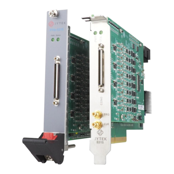
- Page 1 JY5312/5315 Simultaneous Data Acquisition Modules User Manual User Manual Version: V1.5.5 Revision Date: Aug 16, 2022...
-
Page 2: Table Of Contents
3.1 System Requirements ..................13 3.2 System Software .................... 13 3.3 C# Programming Language ................14 3.4 JY5312/5315 Hardware Driver ...............14 3.5 Install the SeeSharpTools from JYTEK ............14 3.6 Running C# Programs in Linux ............... 15 4.Operating JY5312/5315 ..................16 4.1 Quick Start ..................... 16 4.2 Data Acquisition Methods ................ - Page 3 8.Statement ......................47 Table 1 JY5312/5315 Family and Main Features ...........1 Table 2 JY5312/5315 on Different Bus ..............1 Table 3 TB-68 Front Panel for JY5312/5315 Series ..........4 Table 4 Analog Input Specifications ...............5 Table 5 AI Accuracy ....................6 Table 6 AI Bandwidth .....................7 Table 7 CMRR ......................8...
- Page 4 Figure 2 Experiment Setup ..................3 Figure 3 -3dB Bandwidth ..................7 Figure 4 CMRR ....................... 8 Figure 5 JY5312/5315 Front Panel ...............11 Figure 6 AI Simultaneous Mode Acquisition ............17 Figure 7 MultiChannel Continuous Parament ............. 19 Figure 8 Multichannel Continuous Acquisition ........... 19 Figure 9 Differential Mode for Grounding Signal ..........
- Page 5 Figure 37 SSI Connector in PCIe-5312/5315 ............40 Figure 38 DIP Switch in PCIe-5312/5315 ............. 41 Figure 39 Measurement Error ................45 Figure 41 Creating an ����� Return Path ............46 Figure 40 Random Noise ..................45 Figure 42 Gain Error due to Temperature Change ..........47 Figure 43 Offset Error due to Temperature Change ...........
-
Page 6: Overview
1.1 Introduction JY5312/5315 Series Simultaneous DAQ provide 16-channel, 16 bits resolution, up to 5M samples per second per channel. It also has 16 digital IO lines. JY5312/5315 can be run on PCIe, PXIe, TXI(Thunderbolt) and USB bus (coming soon) platforms. -
Page 7: Abbreviations
Programmable Function Interface DIFF: Differential 1.4 Learn by example JYTEK has added Learn by Example in this manual. We provide many sample programs for this device. Please download and install the sample programs for this device. You can visit our web www.jytek.com... - Page 8 Figure 2 Experiment Setup The TB-68 is shown below as Table 3. In the rest of this manual, the wire connection in each Learn by Example section will be given by the pin numbers only. PCIe/PXIe-5310 Series | jytek.com | 3...
- Page 9 Table 3 TB-68 Front Panel for JY5312/5315 Series PCIe/PXIe-5310 Series | jytek.com | 4...
-
Page 10: Hardware Specifications
2. Hardware Specifications 2.1 Analog Input Specifications Table 4 Analog Input Specifications PCIe/PXIe-5310 Series | jytek.com | 5... -
Page 11: Ai Accuracy
Hour or 90 Days accuracy entries. In the case of the 24 Hour column, the accuracy entry becomes (0.0092% of reading + 0.0612% of range). The same 2V measurement now has the accuracy: ± 0.0092% ∗ 2 + 0.0612% ∗ 5 =± 0.003244V =± 3244uV PCIe/PXIe-5310 Series | jytek.com | 6... -
Page 12: Ai Bandwidth
2.4 AI Bandwidth Table 6 AI Bandwidth Figure 3 -3dB Bandwidth PCIe/PXIe-5310 Series | jytek.com | 7... -
Page 13: Cmrr
2.5 CMRR Table 7 CMRR Figure 4 CMRR 2.6 Crosstalk 2.6.1 Adjacent channel Table 8 Crosstalk (Adjacent channel) PCIe/PXIe-5310 Series | jytek.com | 8... -
Page 14: Non-Adjacent Channel
2.6.2 Non-adjacent channel Table 9 Crosstalk (Non-adjacent channel) PCIe/PXIe-5310 Series | jytek.com | 9... -
Page 15: Digital Io Specifications
2.7 Digital IO Specifications Table 10 Digital IO Specifications 2.8 PFI Specifications Table 11 PFI Specifications 2.9 Power Specification Table 12 Power Specification 2.10 Physical and Environment Table 13 Physical and Environment PCIe/PXIe-5310 Series | jytek.com | 10... -
Page 16: Front Panel And Pin Definition
2.11 Front Panel and Pin Definition Figure 5 JY5312/5315 Front Panel JY5312/5315 series are connected to incoming signals by one 68-pin cable for 16 analog input channels and 16 DIO. Table 14 and Table 15 show the pin definition for JY5312/5315 series respectively. - Page 17 Table 14 JY5312/5315 Pin Define Table 15 Notes to Legend PCIe/PXIe-5310 Series | jytek.com | 12...
-
Page 18: Software
Microsoft Windows: Windows 7 32/64 bit, Windows 10 32/64 bit. Linux Kernel Versions: There are many Linux versions. It is not possible JYTEK can support and test our devices under all different Linux versions. JYTEK will at the best support the following Linux versions. -
Page 19: C# Programming Language
3.5 Install the SeeSharpTools from JYTEK To efficiently and effectively use JY5312/5315, you need to install a set of free C# utilities, SeeSharpTools, from JYTEK. The SeeSharpTools offers rich user interface functions you will find convenient in developing your applications. -
Page 20: Running C# Programs In Linux
If you want to use your own Linux development system other than MonoDevelop, you can do it by using our Linux driver. However, JYTEK does not have the capability to support the Linux applications. JYTEK completely relies upon Microsoft to maintain the cross-platform compatibility between Windows and Linux using MonoDevelop. -
Page 21: Operating Jy5312/5315
If you are already familiar with Microsoft Visual Studio C#, the quickest way to use JY5312/5315 is to go through our extensive examples. We provide source code of our examples. In many cases, you can modify the source code and start to write your applications. -
Page 22: Continuous Acquisition
You use the sample program Analog Input --> Winform AI Continuous to learn more about Continuous Acquisition 4.2.2 Finite Acquisition In the Finite Acquisition mode, an AI acquisition task will capture specific number of samples by the parameter, SamplesToAcquire. PCIe/PXIe-5310 Series | jytek.com | 17... -
Page 23: Single Acquisition
Acquisition. Learn by Example 4.2 Connect the two signal source’s positive outputs Ch1, Ch2 to JY5312/5315 AI Ch0 positive (AI0+, Pin#66) and AI Ch1 positive (AI1+, Pin#63), two negative terminals to AI Ch0 negative (AI0-, Pin#32) and AI Ch0 negative (AI1-, Pin#29) as shown in Figure 2 and Table 3. - Page 24 Samples to Acquire is the samples to be acquired for each channel in one block. The continuous mode will acquire blocks after blocks until Stop button is pressed. When Start is clicked, the acquisition starts. The result is shown below. Figure 8 Multichannel Continuous Acquisition PCIe/PXIe-5310 Series | jytek.com | 19...
-
Page 25: Analog Input Terminal Type
(DIFF). In the differential mode you can connect ground-referenced signal to the JY5312/5315. Connect positive side of signal to AI+ terminal, negative side of signal to AI- terminal as shown in Figure 9. Please see the provided software examples for more information. -
Page 26: Trigger Source
The module will acquire the signal immediately after executing the AI Task without any trigger condition setting by default. Learn by Example 4.4.1 Use the same sample program and connection as in Learn by Example 4.2. Figure 11 Immediate Trigger Paraments PCIe/PXIe-5310 Series | jytek.com | 21... -
Page 27: Software Trigger
Learn by Example 4.4.2 Connect the signal source’s positive terminal Ch1 to JY5312/5315 AI Ch0 positive (AI0+, Pin#66), the negative terminal to AI Ch0 negative (AI0-, Pin#32) as shown in Figure 2 and Table 3. (AI0+, AI0-) consists of a DIFF input. -
Page 28: External Analog Trigger
"Falling Slope Trigger": The Edge comparator will output high when the signal go below the threshold. And it will change to low when the signal goes above the threshold as shown in Figure 15. PCIe/PXIe-5310 Series | jytek.com | 23... - Page 29 It will change to low when the signal goes below the low threshold as shown in Figure 16. "Hysteresis with Falling Slope Trigger”: The Hysteresis comparator will output high when the signal must first be above the high threshold, then go below the low PCIe/PXIe-5310 Series | jytek.com | 24...
- Page 30 High Threshold and Low Threshold. There are two trigger conditions. One is acquired the signal inside of the window which is call ed "Entering Window Trigger". Another is acquired the signal outside of the window which is called "Leaving Window Trigger". PCIe/PXIe-5310 Series | jytek.com | 25...
- Page 31 Figure 19 Leaving Window Trigger Learn by Example 4.4.3 Connect the signal source’s positive terminal Ch1 to JY5312/5315 AI Ch0 positive (AI0+, Pin#66), the negative terminal to AI Ch0 negative (AI0-, Pin#32) as shown in Figure 2 and Table 3 TB-68 Front Panel for 5312/5315 Series. (AI0+, AI0-) consists of a DIFF input.
- Page 32 Figure 20 Analog Trigger Paraments Trigger source can be any channel of JY5312/5315 analog input. Set it to Channel_0. Comparators of the Analog Trigger are set by Trigger Comparator. Set it to Edge. Trigger edges (rising/falling) are set by Trigger Edge. Set it to Rising.
-
Page 33: External Digital Trigger
Figure 23. Figure 23 External Digital Trigger PCIe/PXIe-5310 Series | jytek.com | 28... - Page 34 Learn by Example 4.4.4 Connect the signal source’s two positive terminals Ch1, Ch2 to JY5312/5315 AI Ch0 positive (AI0+, Pin#66) and digital trigger source (PFI0, Pin#1), two negative terminals to AI Ch0 negative (AI0-, Pin#32) and the ground for digital operations (DGND, Pin#5) as shown in Figure 2 and Table 3 TB-68 Front Panel for 5312/5315 Series.
- Page 35 Figure 25 Digital Trigger Acquisition Since The squarewave is used for the digital trigger source, when a rising edge of the squarewave occurs, the digital trigger will be activated, and the data acquisition will start. PCIe/PXIe-5310 Series | jytek.com | 30...
-
Page 36: Trigger Mode
4.5 Trigger Mode JY5312/5315 supports several trigger modes: start trigger, reference trigger, and Retrigger. Please see the provided software examples for more information. 4.5.1 Start Trigger In this mode, data acquisition begins immediately after the trigger. This trigger mode is suitable for continuous acquisition and finite acquisition. As shown in Figure 26. -
Page 37: Retrigger
Figure 27 Reference Trigger 4.5.3 ReTrigger JY5312/5315 series modules support retrigger mode. In the retrigger mode, you can set the number of trigger times and the length of each acquisition. Assuming that the number of trigger times is N and the length of each trigger acquisition is M, the length of all acquisition data is N * M * channelcounts as shown in Figure 28. -
Page 38: Learn By Example 4.5
Learn by Example 4.5 Connect the signal source’s positive terminal Ch1 to JY5312/5315 AI Ch0 positive (AI0+, Pin#66), the negative terminal to AI Ch0 negative (AI0-, Pin#32) as shown in Figure 2 and Table 3. (AI0+, AI0-) consists of a DIFF input. - Page 39 Figure 30 Retrigge rIn Start Trigger Mode Now change the Trigger Mode to Reference mode with Pretrigger Sample 1000. A different result is shown below: Figure 31 Retrigger in Reference Trigger Mode PCIe/PXIe-5310 Series | jytek.com | 34...
- Page 40 “3”, then click Start. A message will appear in the lower left corner: “Complete the n trigger”. Figure 32 Retrigger Paraments Figure 33 Retrigger Complete State It shows the acquisition process through every trigger signal. PCIe/PXIe-5310 Series | jytek.com | 35...
-
Page 41: Digital I/O Operations
I/O. User can read these I/O information through software polling. Learn by Example 4.6.1 In this example JY5312/5315 outputs a digital signal by its DO function and reads it back by its DI function. Connect JY5312/5315 Port 0~2’s Line 0~1 to Port 3~5’s Line 0~1. Connections represented in Pins: (Pin1 ... - Page 42 Select all ports for digital input as shown, and click Start. The result is shown below. Figure 35 Single Digital Input The result shows that the digital signals are successfully transferred between Port3~5 and Port 0~2. PCIe/PXIe-5310 Series | jytek.com | 37...
-
Page 43: Multi-Devices Synchronization
4.7 Multi-Devices Synchronization JY5312/5315 Series modules multi-devices synchronization support two methods : ReferenceClockSynchronization and SampelClockSynchronization ReferenceClockSynchronization This method will use 3 signals, Reference clock, Sync Pulse and Triger to achieve data acqusistion simultaneously with multiple modules. First, the master module will notice all of slave modules by routing the trigger signal through PXI trigger bus, PXI_TRIG<0..7>... - Page 44 4. Start all slave tasks. 5. Start the master task (if digital trigger or software trigger is enabled, you need to wait for the trigger signal to arrive), all the tasks will start to work synchronously. PCIe/PXIe-5310 Series | jytek.com | 39...
-
Page 45: System Synchronization Interface(Ssi)For Pcie Modules
4.9 DIP Switch in PCIe-5312/5315 PCIe-5312/5315 series board has a DIP switch. The card number can be adjusted manually by changing the DIP switch setting, which is used to identify the boards with different slot positions. PCIe/PXIe-5310 Series | jytek.com | 40... - Page 46 1 of the DIP switch to the ON position and the orthers to OFF. See below for details. Figure 38 DIP Switch in PCIe-5312/5315 Table 18 Relationship between switch position and slot number PCIe/PXIe-5310 Series | jytek.com | 41...
-
Page 47: Calibration
5. Calibration JY5312/5315 board is precalibrated before the shipment. We recommend you recalibrate your JY5312/5315 board periodically to ensure the measurement accuracy. A commonly accepted practice is one year. If you need to recalibrate your board, please contact JYTEK. PCIe/PXIe-5310 Series | jytek.com | 42... -
Page 48: About Jytek
6. About JYTEK 6.1 JYTEK China Founded in June, 2016, JYTEK China is a leading Chinese test & measurement company, providing complete software and hardware products for the test and measurement industry. The company is a joint venture between Adlink Technologies and a group of experienced professionals form the industry. -
Page 49: Jytek Software Platform
FirmDrive, upon which many our future hardware will be based. In addition to our own developed hardware, JYTEK also rebrands Adlink’s PXI product lines. In addition, JYTEK has other rebranding agreements to increase our hardware coverage. It is our goal to provide the complete product coverage in PXI and PCI modular instrumentation and data acquisition. -
Page 50: System Noise
Figure 39 Measurement Error 7.2 System Noise Table 19 Random Noise Figure 40 Random Noise PCIe/PXIe-5310 Series | jytek.com | 45... - Page 51 In order to eliminate the bias, it is necessary to connect a ground resistance to the channel, and the resistance should be more than 1MΩ. Figure 41 Creating an � ���� Return Path PCIe/PXIe-5310 Series | jytek.com | 46...
-
Page 52: Temperature Drift
Figure 42 Gain Error due to Temperature Change Figure 43 Offset Error due to Temperature Change 8. Statement The hardware and software products described in this manual are provided by JYTEK China, or JYTEK in short. PCIe/PXIe-5310 Series | jytek.com | 47... - Page 53 This manual provides the product review, quick start, some driver interface explanation for JYTEK JY5312/5315 Series family of multi-function data acquisition boards. The manual is copyrighted by JYTEK. No warranty is given as to any implied warranties, express or implied, including any purpose or non-infringement of intellectual property rights, unless such disclaimer is legally invalid.
- Page 54 PCIe/PXIe-5310 Series | jytek.com | 49...
Need help?
Do you have a question about the JY5312 and is the answer not in the manual?
Questions and answers