
Related Manuals for JYTEK USB-61210


Summary of Contents for JYTEK USB-61210
- Page 1 USB-61210 4-CH 16-Bit 2MS/s Simultaneous-Sampling USB DAQ Module User’s Manual Manual Rev.: 1.00 Revision Date: July 31, 2017 Advance Technologies; Automate the World.
- Page 3 Restriction of Hazardous Substances (RoHS) directive and Waste Electri- cal and Electronic Equipment (WEEE) directive. Environmental protec- tion is a top priority for JYTEK. We have enforced measures to ensure that our products, manufacturing processes, components, and raw materials have as liLVTTLe impact on the environment as possible.
- Page 4 Conventions Take note of the following conventions used throughout this manual to make sure that users perform certain tasks and instructions properly. Additional information, aids, and tips that help users perform tasks. NOTE: NOTE: Information to prevent minor physical injury, component damage, data loss, and/or program corruption when trying to complete a task.
-
Page 5: Table Of Contents
Driver Support for Windows............14 1.10 Utilities for Windows ..............14 2 Getting Started ............... 15 Unpacking Checklist ..............15 Attaching the Module Stand............15 Rail Mounting ................16 Wall Mounting ................17 Installing the USB-61210 Module ..........18 Table of Contents... - Page 6 2.5.1 Connecting the USB-61210 Module........18 2.5.2 Device ID ................19 2.5.3 Hardware Configuration............ 20 3 Operation & Calibration ............21 Operation ..................21 3.1.1 Signal Function ..............21 3.1.2 A/D Conversion ..............22 3.1.3 Trigger Sources..............25 3.1.4 Trigger Modes ..............27 3.1.5...
-
Page 7: List Of Figures
Module Rail-Mounted ............17 Figure 2-4: Wall Mount Holes..............17 Figure 2-5: Module with Wall Mount Apparatus.........18 Figure 2-6: USB-61210 module in Windows Device Manager.....19 Figure 2-7: Device ID Selection Control ..........20 Figure 3-1: Carrier Board Functional Block Diagram ......21 Figure 3-2: Daughter Board Functional Block Diagram .......22... - Page 8 Figure 3-20: Mode 7-Single-Triggered Continuous Pulse...... 37 Figure 3-21: Mode 8-Continuous Gated Pulse ........37 Figure 3-22: Mode 9-Edge Separation Measurement......38 Figure 3-23: Mode 10-PWM Output Following Trigger......38 Figure 3-24: Mode 10-PWM Output Following GATE Control ....38 Figure 3-25: Isolation................
- Page 9 List of Tables Table 1-1: USB-61210 Pin Assignment .............11 Table 1-2: CN1/CN2 I/O Signal Description..........12 Table 3-1: Bipolar Analog Input Range and Output Digital Code.....23 Table 3-2: Pin Definition of LVTTL Digital I/O...........31 Table 3-3: Timer/Counter Pin Definition..........32 List of Tables...
- Page 10 This page intentionally left blank. List of Tables...
-
Page 11: Introduction
The USB-61210 is a 16-bit high-speed USB 2.0-based DAQ module equipped with 4 analog input channels providing simultaneous sampling at up to 2MS/s per channel. The USB-61210 delivers high accuracy and excellent dynamic performance at maximum sampling rates and fea- tures flexible trigger function. -
Page 12: General Specifications
1.4.1 General Specifications Digital I/O Specifications Number of channels 8-CH programmable function digital input (DI) 4-CH programmable function digital output (DO) Compatibility LVTTL (single-end) (supports 3.3V and 5 V DI but 3.3V DO) Input voltage Logic low: VIL = 0.8 V max; IIL = 0.2 mA max.Logic high: VIH = 2.0 V min.;... -
Page 13: Analog Input
1.4.2 Analog Input Resolution 16 bit Channels 4 differential (simultaneous sampling) Maximum sampling rate 2MS/s per channel Programmable gain 1, 5 Input range (voltage) ± 10 V, ± 2 V ± 1mV (gain=1) Offset error ± 0.2mV (gain=5) Typical: ± 0.01% of FSR (gain=1 & 5) Gain error Maximum: ±... -
Page 14: Schematics
Programmed I/O, continuous (USB bulk Data transfer transfer mode) Schematics All units are in millimeters (mm) NOTE: NOTE: 1.5.1 Module Figure 1-1: USB-61210 Module Rear View Introduction... -
Page 15: Figure 1-2: Usb-61210 Module Side View
Figure 1-2: USB-61210 Module Side View Introduction... -
Page 16: Figure 1-3: Usb-61210 Module Front View
Figure 1-3: USB-61210 Module Front View Introduction... -
Page 17: Module Stand
1.5.2 Module Stand The multi-function USB-61210 stand is compatible with desk, rail, or wall mounting. To fix the module in the stand, slide the module body into the stand until a click is heard. To remove the module from the stand, twist the bottom of the stand in a back-and forth motion and sep- arate from the module. -
Page 18: Figure 1-5: Module, Stand, & Wall Mount Kit Side View (W/ Connections)
Figure 1-5: Module, Stand, & Wall Mount Kit Side View (w/ connections) Figure 1-6: Module in Stand Front View Introduction... -
Page 19: Figure 1-7: Module Stand Top View
20.4 20.4 Figure 1-7: Module Stand Top View Introduction... -
Page 20: Figure 1-8: Module Stand Side Cutaway View
Figure 1-8: Module Stand Side Cutaway View Figure 1-9: Module Stand Front View Introduction... -
Page 21: Connector Pin Assignment
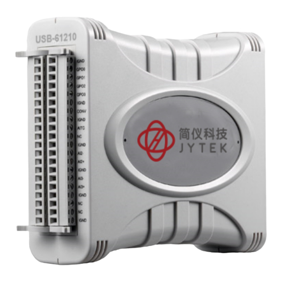
Connector Pin Assignment The USB-61210 module is equipped with 40-pin removable screw-down terminal connectors, with pin assignment as shown. IGND IGND GPI0 GPO0 GPI1 GPO1 GPI2 GPO2 GPI3 GPO3 GPI4 IGND GPI5 CONV GPI6 IGND GPI7 AITG IGND IGND IGND... -
Page 22: Analog Input Signal Connection
A ground-referenced signal is connected in some way to the existing ground system. That is, the signal source is already connected to a common ground point with respect to the USB-61210, assuming that the computer is connected to the same power system. Non-isolated... -
Page 23: Figure 1-10: Grnd-Referenced Source W/ Diff Input
IGND Figure 1-10: GRND-Referenced Source w/ DIFF Input Connection of a floating signal source to the USB-61210 module in differential input mode is further shown. For floating signal sources, the negative side of the signal should be connected to the AIGND, with less noise coupled into the signal connections than in single-end mode. -
Page 24: Software Support
In addition to programming libraries, such as DLLs, for most Windows-based systems, JYTEK also provides drivers for other application environments. Be sure to install the driver & utility before using the USB-61210 mod- ule. Driver Support for Windows... -
Page 25: Getting Started
Retain the shipping carton and packing materials for inspection. Obtain authorization from your dealer before returning any product to JYTEK. Ensure that the following items are included in the package. USB-61210 module ... -
Page 26: Rail Mounting
Rail Mounting The multi-function stand can be mounted on the DIN rail using the rail-mount kit as shown. Figure 2-1: Rail Mount Kit Figure 2-2: Module Pre-Rail Mounting Getting Started... -
Page 27: Wall Mounting
Figure 2-3: Module Rail-Mounted Wall Mounting The multi-function stand can be fixed to a wall using four flush head screws as shown. The four screw holes should be approximately 3.4 mm in diameter. 20.4 13.0 Figure 2-4: Wall Mount Holes Getting Started... -
Page 28: Installing The Usb-61210 Module
2.5.1 Connecting the USB-61210 Module 1. Turn on your computer. 2. Connect the USB-61210 module to one USB 2.0 port on your computer using the included USB cable. 3. The first time the USB-61210 module is connected, a New Hardware message appears. It will take around 6 seconds to load the firmware. -
Page 29: Device Id
Figure 2-6: USB-61210 module in Windows Device Manager If the USB-61210 module cannot be detected, the power provided by the USB port may be insufficient. The USB-61210 module is exclusively powered by the USB port and requires 460 mA @ 5 V. -
Page 30: Hardware Configuration
When more than one USB module of the same type is connected, each must be set to a different ID to avoid conflicts and errors in operation. Figure 2-7: Device ID Selection Control 2.5.3 Hardware Configuration All remaining hardware configurations are software programmable, including sampling/update rate, input/output channel, input range, and others. -
Page 31: Operation & Calibration
Operation & Calibration Operation of the USB-61210 is described here to assist in configuration and programming of the module. Functions described include A/D conversion, programmable function I/O, and others Operation 3.1.1 Signal Function The USB-61210 provides 4 truly differential and simultaneous-sampling analog input channels of 16-bit A/D input. -
Page 32: A/D Conversion
AI CH0+ Signal DC path/ 2nd-order 1st CH AI CH0- Protection Calibration Source SDO_CH0 BUSY_CH0 SDO_CH1 AI CH1+ BUSY_CH1 AI CH1- Four channels SDO_CH2 Calibration BUSY_CH2 Mux and Reference Src AI CH2+ SDO_CH3 BUSY_CH3 AI CH2- 4th CH AI CH3+ Signal DC path/ 2nd-order... -
Page 33: Table 3-1: Bipolar Analog Input Range And Output Digital Code
Analog Input Circuitry 2 MHz ADCONV_CHn Buffer 2nd order Path Selection With Path_DC With level shift x1 or x4 Calibration SRC x1/2 AI CHx_P Signal Input AI CHx_N Signal Input Buffer Figure 3-3: Analog Input AI Data Format The acquired 16-bit A/D data is 2’s complement coded data format. Valid input ranges and ideal transfer characteristics are shown. - Page 34 Continuous A/D Conversion Clock Source When the onboard ADC receives a conversion clock signal, A/D con- version is triggered. The USB-61210 conversion clock may originate with the internal hardware timer or externally via CONV (external A/D conversion clock) pin. While the conversion clock source can be chosen by setting AI source configuration, if precision acquisition is required, use of the internal hardware timer is recommended.
-
Page 35: Trigger Sources
CONV pin. The valid frequency of external clock is from DC to 2 MHz and the minimum pulse width is 225ns. Analog Input Triggering The USB-61210 supports flexible trigger sources for analog input func- tionality. The trigger source can originate with software command, external analog, or external digital signal in continuous analog input mode. -
Page 36: Figure 3-5: Below-Low Analog Triggering
voltage. High_Threshold setting is not used in this triggering situa- tion. Figure 3-5: Below-Low Analog Triggering Above-High Analog Triggering In above-high analog triggering, as shown, the trigger signal is gener- ated when the input analog signal exceeds the High_Threshold volt- age. -
Page 37: Trigger Modes
An external digital trigger occurs when a rising or falling edge is detected on the digital signal connected to the AITG (analog input trigger) pin. Trigger polarity can be programmed using JYTEK software drivers. Signal level of the external digital trigger signals should be LVTTL-compatible, with a minimum pulse of 20ns. -
Page 38: Figure 3-9: Delayed Trigger
Delayed-Trigger Acquisition Mode (no retriggering) Delay-trigger acquisition is indicated when the data collection is to be delayed following the trigger event, as shown. Delay duration is speci- fied by a 32-bit counter value, whereby maximum delay is the period of TIMEBASE X (2 - 1), and minimum delay the period of the timebase. -
Page 39: Figure 3-11: Pre-Trigger
An example is shown, in which N samples of data are acquired after the first trigger signal, after which the USB-61210 awaits the next re-trigger signal (re-trigger signals occurring before the N samples are completed will be ignored). -
Page 40: Programmable Function I/O
Data Figure 3-13: Gated Trigger 3.1.5 Programmable Function I/O The USB-61210 supports powerful programmable I/O function provided by an FPGA chip, configurable as LVTTL DI/DO, 32-bit timer/counters, and PWM output. These signals are single-ended and 5 V LVTTL-compli- ant. LVTTL DI/DO Programmable function I/O can be used as static LVTTL-compliant 8-CH digital input and 4-CH digital output. -
Page 41: Table 3-2: Pin Definition Of Lvttl Digital I/O
N/C* *Not used in DI/O Table 3-2: Pin Definition of LVTTL Digital I/O General Purpose Timer/Counter The USB-61210 is equipped with two general purpose timer/counter sets featuring: Count up/down controllable by hardware or software Programmable counter clock source (internal clock up to 80 MHz, ... -
Page 42: Basic Timer/Counter Function
IGND N/C* *Not used in GPTC Table 3-3: Timer/Counter Pin Definition 3.1.6 Basic Timer/Counter Function Each timer/counter has three inputs that can be controlled via hard- ware or software. They are clock input (GPTC_CLK), gate input (GPTC_GATE), and up/down control input (GPTC_UD). The GPTC_CLK input provides a clock source input to the timer/counter. -
Page 43: Figure 3-14: Mode 1-Simple Gated-Event Calculation
Software start Gate ffff Count value Figure 3-14: Mode 1-Simple Gated-Event Calculation Mode 2: Single Period Measurement The counter calculates the period of the signal on GPTC_GATE in terms of GPTC_CLK. The initial count can be loaded from the software applica- tion. -
Page 44: Figure 3-16: Mode 3-Single Pulse-Width Measurement
cation. After software start, the counter calculates the number of active edges on GPTC_CLK when GPTC_GATE is in its active state. After the completion of the pulse-width interval on GPTC_GATE, GPTC_OUT outputs high and current count value can be read by the software application. -
Page 45: Figure 3-18: Mode 5-Single-Triggered Pulse
Mode 5: Single-Triggered Pulse This mode generates a single pulse with programmable delay and pro- grammable pulse-width following an active GPTC_GATE edge. These programmable parameters can be specified in terms of periods of the GPTC_CLK input. When the first GPTC_GATE edge triggers the single pulse, GPTC_GATE has no effect until software start is executed again. -
Page 46: Figure 3-20: Mode 7-Single-Triggered Continuous Pulse
Mode 7: Single-Triggered Continuous Pulse Generation This mode is similar to Mode 5 except that the counter generates con- tinuous periodic pulses with programmable pulse interval and pulse-width following the first active edge of GPTC_GATE. When the first GPTC_GATE edge triggers the counter, GPTC_GATE has no effect until software start is executed again. -
Page 47: Figure 3-22: Mode 9-Edge Separation Measurement
C o u n t v a l u e Figure 3-22: Mode 9-Edge Separation Measurement Mode 10: PWM Output The USB-61210 timer/counter can also simulate a PWM (Pulse Width Modulation) output. The PWM starts to generate output following a GPTC_GATE edge trigger or being activated/inactivated by the GPTC_GATE high/low logic control. -
Page 48: Isolation
Pulse length 3.1.8 Isolation The USB-61210 provides 500VDC isolation capability to protect against hazardous voltage caused by erroneous signal connection or signal lev- els to be measured exceeding expectation. The isolation circuit can also reduce the ground-loop noise. Figure 3-25: Isolation Calibration 3.2.1... -
Page 49: Loading Calibration Constants
EEPROM. When auto-calibration is complete, the new calibration constants can be saved to the user-configurable banks in the EEPROM. The USB-61210 should be warmed up for at least 15 minutes before initiating auto-calibration NOTE: NOTE:... - Page 50 Operation & Calibration...
-
Page 51: Important Safety Instructions
Important Safety Instructions For user safety, please read and follow all instructions, WARNINGS, CAUTIONS, and NOTES marked in this manual and on the associated equipment before handling/operating the equipment. Read these safety instructions carefully. Keep this user’s manual for future reference. ... - Page 52 Never attempt to fix the equipment. Equipment should only be serviced by qualified personnel. A Lithium-type battery may be provided for uninterrupted, backup or emergency power. Risk of explosion if battery is replaced with an incorrect type; please dispose of used batteries appropriately. WARNING: Equipment must be serviced by authorized technicians ...
-
Page 53: Warranty Policy
For products containing storage devices (hard drives, flash cards, etc.), please back up your data before send- ing them for repair. JYTEK is not responsible for any loss of data. Please ensure the use of properly licensed software with ... - Page 54 2. Our repair service is not covered by JYTEK's guarantee in the following situations: Damage caused by not following instructions in the User's Manual. Damage caused by carelessness on the user's part during product transportation. Damage caused by fire, earthquakes, floods, lightening, ...
-
Page 55: Getting Service
Getting Service Customer satisfaction is our top priority. Contact us should you require any service or assistance. SHANGHAI JYTEK CO.,LTD. Web Site http://www.jytek.com Sales & Service service@jytek.com Telephone No. +86-21-50475899 Fax No. +86-21-50475899 Mailing Address 300 Fang chun Rd., Zhangjiang Hi-Tech... - Page 56 Getting Service...
Need help?
Do you have a question about the USB-61210 and is the answer not in the manual?
Questions and answers