Table of Contents
Advertisement
Quick Links
Advertisement
Table of Contents

Subscribe to Our Youtube Channel
Related Manuals for protech PA-J510


Summary of Contents for protech PA-J510
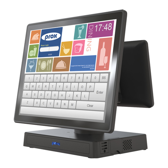
- Page 1 USER MANUAL PA-J510 15" High Performance POS Terminal PA-J510 M3...
- Page 2 PA-J510 15” High Performance POS Terminal COPYRIGHT NOTICE & TRADEMARK All trademarks and registered trademarks mentioned herein are the property of their respective owners. This manual is copyrighted in June 2023. You may not reproduce or transmit in any form or by any means, electronic, or mechanical, including photocopying and recording.
- Page 3 FCC NOTICE This equipment has been tested and found to comply with the limits for a Class A digital device, pursuant to part 15 of the FCC Rules. These limits are designed to provide reasonable protection against harmful interference when the equipment is operated in a commercial environment.
-
Page 4: Table Of Contents
Contents Revision History ..................... v Introduction ..................1-1 About This Manual ..............1-2 Getting Started ..................2-1 Package List ................2-2 System Overview ............... 2-3 2.2.1 Panel PC ................2-3 2.2.2 Normal Stand Only.............. 2-4 2.2.3 Normal Stand with 10.1" 2nd Display ......... 2-5 System Specifications .............. - Page 5 3.5.8 Dual USB 3.0 Ports (USB1) ..........3-12 3.5.9 2nd Display Port (MDP2) ..........3-13 3.5.10 HDMI Port Connector (HDMI1) ......... 3-14 3.5.11 Cash Drawer Port (DRW) ..........3-15 3.5.12 Internal USB Wafer (JUSB1, JUSB9) ....... 3-18 3.5.13 Internal USB Wafer (JUSB7) ..........3-19 3.5.14 M.2 M-Key Connector for SSD (M2_M1) ......
- Page 6 3.8.6 USB 2.0 Connector (JUSB1, JUSB2, JUSB3) ....3-38 3.8.7 Backlight Voltage Selection (JP_INV1) ......3-39 3.8.8 LVDS Panel Voltage Control Selection (JP_VDD1) ..3-39 3.8.9 LVDS Backlight Control (JP1) ........... 3-40 Software Utilities ................. 4-1 Introduction................. 4-2 ® 4.1.1 Installing Intel Chipset Software Installation Utility ...
- Page 7 Appendix A System Diagrams ............ A-1 PPC Memory Maintenance ...............A-2 PPC M.2 2280 Maintenance ..............A-4 PA-J510 Memory Maintenance ..............A-5 PA-J510 M.2 2280 Maintenance ..............A-7 How To Turn System Touchscreen ............A-8 2nd Display Assembly ................A-9 VFD Module Assembly ................A-12 iButton Module Assembly ...............A-14 Fingerprint Module Assembly ..............A-15...
-
Page 8: Revision History
Revision History The revision history of PA-J510 User Manual is described below: Version No. Revision History Date Added: The default voltage of Cash Drawer 2023/6/15 is “default at +24V”. (Page 2-6) The description of Section 3.5.11 Cash Drawer 2023/4/25 Port (DRW) has been revised. (Page 3-15) -
Page 9: Introduction
Introduction This chapter provides the introduction for PA-J510 system as well as the framework of the user manual. The following topic is included: • About This Manual Page: 1-1 PA-J510 SERIES USER MANUAL... -
Page 10: About This Manual
1.1 About This Manual 1.1 About This Manual Thank you for purchasing our PA-J510 system. The PA-J510 is an updated system designed to be comparable with the highest performance of IB M AT personal computers. The PA-J510 provides faster processing speed, greater expandability and can handle more tasks than before. -
Page 11: Getting Started
Getting Started This chapter provides the introduction for the PA-J510 system as well as the framework of the user manual. The following topic is included: • About This Manual • POS System Illustration • System Specifications • Safety precautions Experienced users can jump to Chapter 3 on page 3-1 for a quick start. -
Page 12: Package List
2.1 Package List If you discover any of the items listed below are damaged or lost, please contact your local distributor immediately. Item Q’ty PA-J510 POS System Manual / Driver DVD Power Adapter Power Cord PA-J510 Series User Manual Page: 2-2... -
Page 13: System Overview
Chapter 2 Getting Started 2.2 System Overview Unit: mm 2.2.1 Panel PC Front View Rear View VESA 75 Side View 60.4 24.4 PA-J510 Series User Manual Page: 2-3... -
Page 14: Normal Stand Only
Chapter 2 Getting Started 2.2.2 Normal Stand Only Unit: mm Front View Rear View Type C HDMI DC In LAN COM2 COM1 DRW 1st Dis. 2nd Dis. Side View 24.4 PA-J510 Series User Manual Page: 2-4... -
Page 15: Normal Stand With 10.1" 2Nd Display
Chapter 2 Getting Started 2.2.3 Normal Stand with 10.1" 2nd Display Unit: mm Front View Rear View Type C HDMI DC In LAN COM2 COM1 DRW 1st Dis. 2nd Dis. Side View 198.8 24.4 20.2 PA-J510 Series User Manual Page: 2-5... -
Page 16: System Specifications
VESA 75 x 75mm standard Storage SATA 1 x M.2 2280, SATA interface I/O Ports 1 x Mini DP for Primary display (for Protech original display only) Display 1 x Mini DP for 2nd display (for Protech original display only) ... - Page 17 0~50 degree Environment EMC & Safety CE / FCC Operating Temp. 0°C ~ 35°C (32°F ~ 95°F) Storage Temp. -20°C ~ 60°C (-4°F ~ 140°F) Humidity 20% ~ 90% PA-J510 Series User Manual Page: 2-7...
-
Page 18: Safety Precautions
Avoid direct sunlight exposure for a long period of time (for example, in a closed car in summer time. Also avoid the system from any heating device.). Or do not use PA-J510 when it has been left outdoors in a cold winter day. •... -
Page 19: System Configuration
System Configuration This chapter provides the information for the PA-J510 system. It describes the jumper and connector settings, component locations, and pin assignment. The following topics are included: • System External I/O Port Diagram • Mainboard Component Locations & Jumper Setting •... -
Page 20: System External I/O Ports Diagram
Type C USB 3.0 DC OUT Power USB Side I/O Open up the cover from the right side of PA-J510 Box as shown and find the Side I/O USB7 and Power Button. USB7 Power Button PA-J510 Series User Manual Page: 3-2... -
Page 21: Mainboard Component Locations & Jumper Setting
JUSB7 M.2 E Key M.2 M Key USB7 M2_M2 M2_E1 JCMOS1 JRST1 JUSB1 JBAT1 HDMI1 DC_IN1 USB-C MDP2 MDP1 USB2 USB1 LAN1 DRW1 COM2 COM1 COM2 COM1 HDMI MDP1 MDP2 DC IN Type C PA-J510 Series User Manual Page: 3-3... -
Page 22: How To Set Jumpers
PIN1 and PIN2 to create one setting and shorting. You can also select to connect PIN2 and PIN3 to create another setting. The same jumper diagrams are applied all through this manual. The figure below shows what the manual diagrams look and what they represent. PA-J510 Series User Manual Page: 3-4... - Page 23 Chapter 3 System Configuration Jumper diagrams Jumper settings PA-J510 Series User Manual Page: 3-5...
-
Page 24: Main Board Connector & Jumper Quick Reference Table
Power Output 24V Wafer 24V_OUT1 System LED Wafer JSYS_LED1 CPU FAN Wafer CPU_FAN1 Power Button Wafer JPWRBTN1 Battery Wafer JBAT1 System Reset Wafer JRST1 M.2 M-Key Connector for SSD M2_M1, M2_M2 M.2 E-Key Connector for Wi-Fi M2_E1 PA-J510 Series User Manual Page: 3-6... -
Page 25: Setting Main Board Connectors And Jumpers
3.5 Setting Main Board Connectors and Jumpers 3.5.1 Power Switch Connector Location: Power Switch Description: To turn on the system, open up the cover from the right side of PA-J510 Box and press the power switch briefly. ACTION ASSIGNMENT Click Release +3.3V... -
Page 26: 1St Display Port (Mdp1)
Chapter 3 System Configuration 3.5.3 1st Display Port (MDP1) Connector Location: MDP1 Description: 1st Display Port Proprietary Pin Assignment for Protech Original Display Only: ASSIGNMENT EDP_HPD_C_A DDIA_LANE0_DP_C EDP_BKLT_EN_R DDIA_LANE0_DN_C EDP_BKLT_CTRL_R MDP1 EDP_VDD_EN_R DDIA_LANE1_DP_C USB2_P3_DN_C DDIA_LANE1_DN_C USB2_P3_DP_C HD_GND LINE-OUT-R DDIA_AUX_DP_C LINE-OUT-L... -
Page 27: Com Ports (Com1, Com2)
The voltage of external ports "COM1 and COM2" is made to control on BIOS for your convenience. Please refer to the descriptions of Serial Port 1 and Serial Port 2 Configuration under Advanced > F81967 Super IO Configuration menu in Chapter 5 BIOS Setup. PA-J510 Series User Manual Page: 3-9... -
Page 28: Lan Port (Lan1)
LAN1_MDI3_DP LAN1_MDI3_DN LAN1 LAN LED Indicator: Left Side LED Orange Color Blinking Giga LAN Message Active Green Color Blinking 10/100Mbps LAN Message Active Right Side LED Green Color On LAN switch / hub connected. PA-J510 Series User Manual Page: 3-10... -
Page 29: Usb Type C Port (Usb Type C)
USB Type C Port (USB Type C) Connector Location: USB Type C Description: USB Type C USB Type C ASSIGNMENT ASSIGNMENT USB31_P3_TX_DP_R USB31_P4_TX_DP_R USB31_P3_TX_DN_R USB31_P4_TX_DN_R TYPEC_PWR TYPEC_PWR USB2_P4_DP_R USB2_P4_DP_R USB2_P4_DN_R USB2_P4_DN_R TYPEC_PWR TYPEC_PWR USB31_P4_RX_DN_R USB31_P3_RX_DN_R USB31_P4_RX_DP_R USB31_P3_RX_DP_R PA-J510 Series User Manual Page: 3-11... -
Page 30: Dual Usb 2.0 Ports (Usb2)
Dual USB 3.0 Ports (USB1) Connector Location: USB1 Description: USB 3.0 Type A Ports USB 3.0 ASSIGNMENT ASSIGNMENT USB_PWR1 USB_PWR2 USB2_P1_DN USB2_P2_DN USB2_P1_DP USB2_P2_DP USB31_P1_RX_DN USB31_P2_RX_DN USB31_P1_RX_DP USB31_P2_RX_DP USB1 USB31_P1_TX_DN USB31_P2_TX_DN (USB3.0) USB31_P1_TX_DP USB31_P2_TX_DP PA-J510 Series User Manual Page: 3-12... -
Page 31: 2Nd Display Port (Mdp2)
Chapter 3 System Configuration 3.5.9 2nd Display Port (MDP2) Connector Location: MDP2 Description: 2nd Display Port Proprietary Pin Assignment for Protech Original Display Only: ASSIGNMENT EDP_HPD_C_B DDIB_LANE0_DP_C 2ND_BKLT_EN DDIB_LANE0_DN_C 2ND_BKLT_CTRL MDP2 2ND_VDD_EN DDIB_LANE1_DP_C USB2_P6_DN_C DDIB_LANE1_DN_C USB2_P6_DP_C DDIB_AUX_DP_C DDIB_AUX_DN_C V24P0 PA-J510 Series User Manual... -
Page 32: Hdmi Port Connector (Hdmi1)
Chapter 3 System Configuration 3.5.10 HDMI Port Connector (HDMI1) Connector Location: HDMI1 Description: Display Port Connector HDMI1 ASSIGNMENT ASSIGNMENT HDMI_P2 HDMI_N2 HDMI_P1 HDMI_N1 HDMI_P0 HDMI_N0 HDMI_CLKP HDMI_CLKN HDMI_SCL_5V HDMI_SDA_5V V5P0S_HDM HDMI_HPD PA-J510 Series User Manual Page: 3-14... -
Page 33: Cash Drawer Port (Drw)
2E (hex), then write/read data to/from the assigned register through data port 2F (hex). SIO Address LDN06, Cash drawer Open 0x81, bit1 LDN06, Cash drawer Status 0x81, bit0 PA-J510 Series User Manual Page: 3-15... - Page 34 To exit the Extended Function Mode, writing 0xAA to the EFER is required. Once the chip exits the Extended Function Mode, it is in the normal running mode and is ready to enter the configuration mode. PA-J510 Series User Manual Page: 3-16...
- Page 35 ; ------------------------- Enter to extended function mode ------------------------------- ; ----------------------- Select Logical Device 6 of Cash Drawer --------------------- ;---------------------------------Open the Cash Drawer ------------------------------ ;---------------------------------Close the Cash Drawer ------------------------------ ;---------------------------------Exit the extended function mode ------------------------- PA-J510 Series User Manual Page: 3-17...
-
Page 36: Internal Usb Wafer (Jusb1, Jusb9)
Chapter 3 System Configuration 3.5.12 Internal USB Wafer (JUSB1, JUSB9) Connector Location: JUSB1, JUSB9 Description: Internal USB Wafer JUSB1 ASSIGNMENT USB_PWR9 USB2_P9_DN JUSB1 USB2_P9_DP JUSB9 ASSIGNMENT USB_PWR9 USB2_P9_DN USB2_P9_DP JUSB9 PA-J510 Series User Manual Page: 3-18... -
Page 37: Internal Usb Wafer (Jusb7)
Chapter 3 System Configuration 3.5.13 Internal USB Wafer (JUSB7) Connector Location: JUSB7 Description: Internal USB Wafer (Co-lay with side I/O USB7) JUSB7 ASSIGNMENT JUSB7 PA-J510 Series User Manual Page: 3-19... -
Page 38: M-Key Connector For Ssd (M2_M1)
Description: M.2 M-Key Connector for SSD M2_M1 ASSIGNMENT ASSIGNMENT V3P3S_M2_CPU V3P3S_M2_CPU PCIE4_RX_N3 PCIE4_RX_P3 M2_LED1 V3P3S_M2_CPU PCIE4_TX_N3 V3P3S_M2_CPU PCIE4_TX_P3 V3P3S_M2_CPU V3P3S_M2_CPU PCIE4_RX_N2 PCIE4_RX_P2 PCIE4_TX_N2 PCIE4_TX_P2 PCIE4_RX_N1 PCIE4_RX_P1 PCIE4_TX_N1 PCIE4_TX_P1 PCIE4_RX_N0_SATA1_RXP PCIE4_RX_P0_SATA1_RXN PCIE4_TX_N0_SATA1_TXN M2_KEYM_CPU_SSD_RST_R_N PCIE4_TX_P0_SATA1_TXP GPPC_D5_SRCCLKREQ0_N WAKE_N CLK_SRC0_DN PA-J510 Series User Manual Page: 3-20... - Page 39 Chapter 3 System Configuration ASSIGNMENT ASSIGNMENT CLK_SRC0_DP M_KEY M_KEY M_KEY M_KEY V3P3S_M2_CPU PCIE_SEL V3P3S_M2_CPU V3P3S_M2_CPU PA-J510 Series User Manual Page: 3-21...
- Page 40 M.2 M-Key Connector for SSD (M2_M2) Connector Location: M2_M2 Description: M.2 M-Key Connector for SSD M2_M1 ASSIGNMENT ASSIGNMENT V3P3S_M2_CPU V3P3S_M2_CPU M2_LED2 V3P3S_M2_CPU V3P3S_M2_CPU V3P3S_M2_CPU V3P3S_M2_CPU PCIE4_RX_N1 SATA_0_RX_DP SATA_0_RX_DN SATA_0_TX_DN M2_KEYM_CPU_SSD_RST_R_N SATA_0_TX_DP GPPC_D5_SRCCLKREQ0_N WAKE_N CLK_SRC1_DN PA-J510 Series User Manual Page: 3-22...
- Page 41 Chapter 3 System Configuration ASSIGNMENT ASSIGNMENT CLK_SRC1_DP M_KEY M_KEY M_KEY M_KEY V3P3S_M2_1 V3P3S_M2_1 V3P3S_M2_1 PA-J510 Series User Manual Page: 3-23...
-
Page 42: E-Key Connector For Wi-Fi (M2_E1)
CNV_RF_RESET_N CNVI_WR_D1N CNVI_WR_D1P CRF_XTAL_CLKREQ M.2_BT_LED2_N CNVI_WR_D0N CNVI_WR_D0P CNV_BRI_RSP CNVI_WR_CLKN E-KEY CNVI_WR_CLKP E-KEY E-KEY E-KEY E-KEY E-KEY E-KEY CNV_RGI_DT E-KEY CNV_RGI_RSP CNV_BRI_DT PCIE3_P10_UFS_11_TX_DP MLK_RST_N PCIE3_P10_UFS_11_TX_DN MLK_DATA MLK_CLK PCIE3_P10_UFS_11_RX_DP PCIE3_P10_UFS_11_RX_DN CLK_SRC5_DP SUS_CLK CLK_SRC5_DN M.2_WLAN_PERST_R_N GPPC_A13_BT_RF_KILL_N GPPC_H11_SRCCLKREQ5_N PA-J510 Series User Manual Page: 3-24... - Page 43 Chapter 3 System Configuration ASSIGNMENT ASSIGNMENT GPPC_B15_WIFI_RF_KILL_N GPPC_C23_WIFI_WAKE_N CNVI_WT_D1N CNVI_WT_D1P TP11 CNVI_WT_D0N CNVI_WT_D0P V3.3A_WLAN CNVI_WT_CLKN V3.3A_WLAN CNVI_WT_CLKP PA-J510 Series User Manual Page: 3-25...
-
Page 44: Speaker Wafer (Jspk1)
VOUTN JSPK1 3.5.18 Microphone Connector (JMIC1) Connector Location: JMIC1 Description: Mic Pin Header ASSIGNMENT HD_MIC1-R_L HD_GND HD_MIC1-L_L JMIC1 3.5.19 Power Output 24V Wafer (J24V_OUT1) Connector Location: J24V_OUT1 Power Output 24V Wafer Description: ASSIGNMENT J24V_OUT1 PA-J510 Series User Manual Page: 3-26... -
Page 45: System Led Wafer (Jsys_Led1)
Chapter 3 System Configuration 3.5.20 System LED Wafer (JSYS_LED1) Connector Location: JSYS_LED1 Wafer Description: System LED ASSIGNMENT V5P0 JSYS_LED1 3.5.21 CPU Fan Wafer (CPU_FAN1) Connector Location: CPU_FAN1 Description: CPU Fan Wafer ASSIGNMENT V12P0 sense CPU_FAN1 Control PA-J510 Series User Manual Page: 3-27... -
Page 46: Power Button Wafer (Jpwrbtn1)
Description: Power Button Wafer ASSIGNMENT V3P3A JPWRBTN1 3.5.23 Battery Wafer (JBAT1) Connector Location: JBAT1 Description: Battery Wafer ASSIGNMENT VRTC_BATT JBAT1 3.5.24 System Reset Wafer (JRST1) Connector Location: JRST1 Description: System Reset Wafer ASSIGNMENT RST_SW JRST1 PA-J510 Series User Manual Page: 3-28... -
Page 47: Usb Signal Selection (Jp1)
(Default Setting) (for M2_E1) JUSB1-USB2.0 D+ (for JUSB1) 3.5.26 USB Signal Selection (JP2) Jumper Location: JP2 Description: USB Signal Selection SELECTION JUMPER SETTING JUMPER ILLUSTRATION M2_E1-USB2.0 D- (for M2_E1) (Default Setting) JUSB1-USB2.0 D- (for JUSB1) PA-J510 Series User Manual Page: 3-29... -
Page 48: Cash Drawer Voltage Selection (Jp3)
Chapter 3 System Configuration 3.5.27 Cash Drawer Voltage Selection (JP3) Jumper Location: JP3 Description: Cash Drawer Voltage Selection SELECTION JUMPER SETTING JUMPER ILLUSTRATION (Default Setting) PA-J510 Series User Manual Page: 3-30... -
Page 49: Clear Cmos Data Selection (Jpcmos1)
Note: To clear CMOS data, you must power off the computer and set the jumper to “Clear CMOS” as illustrated above. After five to six seconds, set the jumper back to “Normal” and power on the computer. PA-J510 Series User Manual Page: 3-31... -
Page 50: A/D Board Component Locations & Jumper Setting
Chapter 3 System Configuration 3.6 A/D Board Component Locations & Jumper Setting A/D Board: PR-J500 JSPK1 MDP1 JEDP2 JP_VDD1 JP_INV1 LVDS1 JUSB1 JUSB3 JUSB2 PA-J510 Series User Manual Page: 3-32... -
Page 51: A/D Board Connector & Jumper Quick Reference Table
LVDS Panel Voltage Selection JP_VDD1 LVDS Backlight Control CONNECTOR NAME 1st Display Port Connector MDP1 Embedded DisplayPort JEDP2 Connector Speaker Connector JSPK1 Inverter Connector JINV1 LVDS Connector LVDS1 USB 2.0 Connector JUSB1, JUSB2, JUSB3 PA-J510 Series User Manual Page: 3-33... -
Page 52: Setting A/D Board Connectors And Jumpers
Chapter 3 System Configuration 3.8 Setting A/D Board Connectors and Jumpers 3.8.1 1st Display Port Connector (MDP1) Connector Location: MDP1 Description: 1st Display Port Connector Proprietary Pin Assignment for Protech Original Display Only: ASSIGNMENT EDP_HPD_C_A DDIA_LANE0_DP_C EDP_BKLT_EN_R DDIA_LANE0_DN_C EDP_BKLT_CTRL_R MDP1... -
Page 53: Embedded Displayport Connector (Jedp2)
Embedded DisplayPort Connector (JEDP2) Connector Location: JEDP2 Description: Embedded DisplayPort Connector JEDP2 ASSIGNMENT ASSIGNMENT LVDS_VDD EDP_SELF_TEST EDP_HPD NGND EDP_LANE1_DN_C EDP_LANE1_DP_C EDP_LANE0_DN_C EDP_BKLT_EN EDP_LANE0_DP_C DP_BKLT_CTRL EDP_DCR_EN EDP_AUX_DN_C EDP_AUX_DP_C INV_VCC INV_VCC LVDS_VDD INV_VCC LVDS_VDD INV_VCC LVDS_VDD PA-J510 Series User Manual Page: 3-35... -
Page 54: Speaker Connector (Jspk1)
Chapter 3 System Configuration 3.8.3 Speaker Connector (JSPK1) Connector Location: JSPK1 Description: Speaker Connector ASSIGNMENT VOUTP VOUTN JSPK1 3.8.4 Inverter Connector (JINV1) Connector Location: JINV1 Description: Inverter Connector ASSIGNMENT INV_VCC INV_VCC LVDS_BKLCTL JINV1 LVDS_BKLTEN PA-J510 Series User Manual Page: 3-36... -
Page 55: Lvds Connector (Lvds1)
LVDS Connector (LVDS1) Connector Location: LVDS1 Description: LVDS Connector ASSIGNMENT ASSIGNMENT LVDS_VDD LVDS_CLKB_DN LVDS_CLKB_DP LVDS_B2_DN LVDS_B2_DP LVDS_B1_DN LVDS_B1_DP LVDS_B3_DP LVDS_B3_DN LVDS_B0_DP LVDS_B0_DN LVDS_CLKA_DP LVDS_CLKA_DN LVDS_A2_DP LVDS_A2_DN LVDS_A1_DP LVDS_A1_DN LVDS_A0_DP LVDS_A0_DN LVDS1 LVDS_A3_DP LVDS_A3_DN LVDS_VDD LVDS_VDD PA-J510 Series User Manual Page: 3-37... -
Page 56: Usb 2.0 Connector (Jusb1, Jusb2, Jusb3)
USB 2.0 Connector (JUSB1, JUSB2, JUSB3) Connector Location: JUSB1, JUSB2, JUSB3 Description: USB 2.0 Connector JUSB1 ASSIGNMENT ASSIGNMENT V5P0S_USB2 V5P0S_USB1 HUB1_DN2 HUB1_DN1 HUB1_DP2 HUB1_DP1 JUSB1 JUSB2 ASSIGNMENT V5P0S_USB3 HUB1_DN3 HUB1_DP3 JUSB2 JUSB3 ASSIGNMENT V5P0S_USB4 HUB1_DN42 HUB1_DP42 JUSB3 PA-J510 Series User Manual Page: 3-38... -
Page 57: Backlight Voltage Selection (Jp_Inv1)
(Default Setting) (VIN_INV) JP_INV1 (VIN_INV) JP_INV1 3.8.8 LVDS Panel Voltage Control Selection (JP_VDD1) Jumper Location: JP_VDD1 LVDS Panel Voltage Control Selection Description: SELECTION JUMPER SETTING JUMPER ILLUSTRATION 3.3V (LVDS_VDD) (Default Setting) JP_VDD1 (LVDS_VDD) JP_VDD1 PA-J510 Series User Manual Page: 3-39... -
Page 58: Lvds Backlight Control (Jp1)
Chapter 3 System Configuration 3.8.9 LVDS Backlight Control Selection (JP1) Jumper Location: JP1 LVDS Backlight Control Selection Description: SELECTION JUMPER SETTING JUMPER ILLUSTRATION 3.3V (LVDS_BKLCTL) (Default Setting) (LVDS_BKLCTL) PA-J510 Series User Manual Page: 3-40... -
Page 59: Software Utilities
Chipset Software Installation Utility • Installing Graphics Driver Utility ® • Installing Intel Management Engine Components Driver Installer • Installing LAN Driver Utility • Installing Intel Serial I/O Driver Utility ® • Installing Sound Driver Utility PA-J510 Series User Manual Page 4-1... - Page 60 Chapter 4 Software 4.1 Introduction Enclosed with the PA-J510 Series package is our driver utilities, which comes in a DVD-ROM format. Refer to the following table for driver locations Windows 10 Enterprise 2016 LTSB_64Bit Filename (Assume that Purpose DVD- ROM drive is D :)
- Page 61 The utility pack is to be installed only for Windows 10 64Bit, and it should be installed immediately after the OS installation is finished. Please follow the steps below: Connect the USB DVD-ROM device to PA-J510 and insert the driver disk. Enter the “Main Chip” folder where the Chipset driver is located.
- Page 62 Chapter 4 Software 4.1.2 Installing Graphics Driver Utility The GRAPHICS interface embedded in PA-J510 can support a wide range of display types. You can have dual displays via LCD and LVDS interfaces and make the system work simultaneously. To install the Graphics driver utility, follow the steps below: Connect the USB DVD-ROM device to PA-J510 and insert the driver disk.
- Page 63 Intel Management Engine Components Installer Installation To install the ME Driver, follow the steps below: Connect the USB DVD-ROM device to PA-J510 and insert the driver disk Enter the “ME” folder where the driver is located Click “SetupME.exe” file for driver installation.
- Page 64 Once the installation is completed, shut down the system and restart PA-J510 for the changes to take effect. For more details on the installation procedure, refer to the Readme.txt file that you can find on LAN Driver Utility.
- Page 65 Installing Intel Serial I/O Driver Utility To install the Serial I/O Driver, follow the steps below: Connect the USB DVD-ROM device to PA-J510 and insert the driver disk. Open the “Serial IO” folder where the driver is located. Click the “SetupSerialIO.exe” file for driver installation.
- Page 66 The sound function enhanced in this system is fully compatible with Windows 10. To install the Sound Driver, follow the steps below: Connect the USB DVD-ROM device to PA-J510 and insert the driver disk. Open the “sound” folder where the driver is located.
-
Page 67: Bios Setup
The BIOS Setup Utilities consist of the following menu items: Main Menu • Advanced Menu • Chipset Menu • Security Menu • Boot Menu • Save & Exit Menu • PA-J510 Series User Manual Page 5-1... -
Page 68: Introduction
Chapter 5 BIOS Setup 5.1 Introduction The PA-J5 0 uses an AMI Aptio BIOS that is stored in the Serial Peripheral Interface Flash Memory (SPI Flash) and can be updated. The SPI Flash contains the BIOS Setup program, Power-on Self-Test (POST), the PCI auto-configuration utility, LAN EEPROM information, and Plug and Play support. - Page 69 Chapter 5 BIOS Setup The BIOS Setup program can be used to view and change the BIOS settings for the computer. The BIOS Setup program is accessed by pressing the <Del> or <ESC> key after the POST memory test begins and before the operating system boot begins. The settings are shown below.
-
Page 70: Accessing Setup Utility
Chapter 5 BIOS Setup 5.1.1.1 Accessing Setup Utility When the system is powered on, the BIOS will enter the Power-On Self Test (POST) routines and the following message will appear on the lower screen: POST Screen with AMI Logo As long as this message is present on the screen you may press the <Del> key (the one that shares the decimal point at the bottom of the number keypad) to access the Setup program. - Page 71 Chapter 5 BIOS Setup BIOS Setup Menu Initialization Screen You may move the cursor by up/down keys to highlight the individual menu items. As you highlight each item, a brief description of the highlighted selection will appear at the bottom of the screen. The language of the BIOS setup menu interface and help messages are shown in US English.
- Page 72 Chapter 5 BIOS Setup BIOS Setup Navigation Key Description Select a different menu screen (move the cursor from <←> and <→> the selected menu to the left or right). Select a different item (move the cursor from the <↑> and <↓> selected item upwards or downwards) <Enter>...
-
Page 73: Main
Chapter 5 BIOS Setup 5.1.2 Main Menu Path Main The Main menu allows you to view the BIOS Information and change the system date and time. Use tab to switch between date elements. Use <↑> or <↓> arrow keys to highlight the item and enter the value you want in each item. This screen also displays the BIOS version (project) and BIOS Build Date and Time. -
Page 74: Advanced
Chapter 5 BIOS Setup BIOS Setting Options Description/Purpose Stepping No changeable options Displays the stepping of the PCH Sets the current date. The format is [Day Month/Date/ Year]. Users can directly enter System Date month, day, year values or use <+> or <-> arrow keys to increase/decrease it. - Page 75 Chapter 5 BIOS Setup BIOS Setting Options Description/Purpose CPU Configuration CPU Configuration Parameters. Sub-Menu Management Engine Technology PCH-FW Configuration Sub-Menu Parameters. Trusted Computing Trusted Computing Settings. Sub-Menu ACPI Settings System ACPI Parameters. Sub-Menu F81967 Super IO System Super IO Chip parameters. Sub-Menu Configuration Hardware Monitor...
-
Page 76: Advanced - Cpu Configuration
Chapter 5 BIOS Setup 5.1.3.1 Advanced - CPU Configuration Menu Path Advanced > CPU Configuration The CPU Configuration provides advanced CPU settings and some information about CPU. CPU Configuration Screen BIOS Setting Options Description/Purpose Type No changeable options Displays the CPU Type. No changeable options Displays the CPU ID. -
Page 77: Advanced - Pch-Fw Configuration
Chapter 5 BIOS Setup BIOS Setting Options Description/Purpose SMX/TXT No changeable options Secure Mode extensions support. Intel (VMX) When enabled, VMM can utilize the - Disabled Virtualization additional hardware capabilities provided - Enabled (Default) Technology by Vanderpool Technology - Disabled When Disabled, only one thread per Hyper-Threading - Enabled (Default) - Page 78 Chapter 5 BIOS Setup Advanced - PCH-FW Configuration - PTT Configuration Menu Path Advanced > PCH-FW Configuration > PTT Configuration PTT Configuration Screen BIOS Setting Options Description/Purpose - PTT (Default) TPM Device Selection Selects TPM device: PTT or dTPM. - dTPM PA-J5 0 Series User Manual Page 5-12...
-
Page 79: Advanced - Trusted Computing
Chapter 5 BIOS Setup 5.1.3.3 Advanced - Trusted Computing Menu Path Advanced > Trusted Computing The Trusted Computing allows users to enable / disable BIOS support for security device. The operating system will now show Security Device. The TCG EFI protocol and INT1A interface will not be available. - Page 80 Chapter 5 BIOS Setup BIOS Setting Options Description/Purpose - Enabled (Default) - Disabled (Default) SHA384 PCR Bank Enables or Disables SHA384 PCR Bank. - Enabled - Disabled (Default) Enables or Disables SM3_256 PCR SM3_256 PCR Bank - Enabled Bank. Schedules an Operation for the Security - None (Default) Device.
-
Page 81: Advanced - Acpi Settings
Chapter 5 BIOS Setup 5.1.3.4 Advanced - ACPI Settings Menu Path Advanced > ACPI Settings The ACPI Settings allows users to configure relevant ACPI (Advanced Configuration and Power Management Interface) settings, such as enable / disable ACPI Auto Configuration, enable / disable Hibernation, ACPI Sleep State and S3 Video Repost. -
Page 82: Advanced - F81967 Super Io Configuration
Chapter 5 BIOS Setup 5.1.3.5 Advanced - F81967 Super IO Configuration Menu Path Advanced > F81967 Super IO Configuration The F81967 Super IO Configuration allows users to configure the serial ports 1-2. F81967 Super IO Configuration Screen BIOS Setting Options Description/Purpose Configure the parameters of Serial Port 1 Serial Port 1 Configuration... - Page 83 Chapter 5 BIOS Setup F81967 Super IO Configuration – Serial Port 1 Configuration Menu Path Advanced > F81967 Super IO Configuration > Serial Port 1 Configuration Serial Port 1 Configuration Screen BIOS Setting Options Description/Purpose - Disabled Serial Port Enables or disables Serial Port 1. - Enabled (Default) Displays the current settings of Device Settings...
- Page 84 Chapter 5 BIOS Setup F81967 Super IO Configuration – Serial Port 2 Configuration Menu Path Advanced > F81967 Super IO Configuration > Serial Port 2 Configuration Serial Port 2 Configuration Screen BIOS Setting Options Description/Purpose - Disabled Serial Port Enables or disables Serial Port 2. - Enabled Displays the current settings of Device Settings...
-
Page 85: Advanced - Hardware Monitor
BIOS Setting Options Description/Purpose Smart Fan Mode Smart Fan Mode Selection. Sub-Menu Configuration Note: No CPU Fan is used on PA-J510. CPU temperature No changeable options Displays the processor's temperature. System temperature No changeable options Displays the system's temperature. Displays CPU Fan speed. - Page 86 Chapter 5 BIOS Setup BIOS Setting Options Description/Purpose Detects and displays the voltage level of VCC3V No changeable options VCC3V in supply. Detects and displays the voltage level of VSB3V No changeable options VSB3V in supply. Detects and displays the voltage level of VCC5V No changeable options VCC5V in supply.
- Page 87 Chapter 5 BIOS Setup Smart Fan Mode Configuration Menu Path Advanced > Hardware Monitor > Smart Fan Mode Configuration Smart Fan Mode Configuration Screen BIOS Setting Options Description/Purpose CPU Fan Smart Fan - Manual Duty Mode Smart Fan Mode select for CPU Fan. Control - Auto Duty-Cycle Mode Manual mode fan control, user can...
-
Page 88: Advanced - F81967 Watchdog
Chapter 5 BIOS Setup 5.1.3.7 Advanced - F81967 Watchdog Menu Path Advanced > F81967 Watchdog If the system hangs or fails to respond, enable the F81967 watchdog function to trigger a system reset via the 255-level watchdog timer. F81967 Watchdog Screen BIOS Setting Options Description/Purpose... -
Page 89: Advanced - Usb Configuration
Chapter 5 BIOS Setup 5.1.3.8 Advanced - USB Configuration Menu Path Advanced > USB Configuration The USB Configuration allows users to configure advanced USB settings such as USB mass storage driver support. USB Configuration Screen BIOS Setting Options Description/Purpose USB Module No changeable options Displays USB module version. -
Page 90: Advanced - Nvme Configuration
Chapter 5 BIOS Setup 5.1.3.9 Advanced - NVMe Configuration Menu Path Advanced > NVMe Configuration The NVMe Configuration allows users to view the information about NVMe Device. NVMe Configuration Screen BIOS Setting Options Description/Purpose NVMe Configuration No changeable options Displays NVMe device. PA-J5 0 Series User Manual Page 5-24... -
Page 91: Chipset
Chapter 5 BIOS Setup 5.1.4 Chipset Menu Path Chipset This menu allows users to configure advanced Chipset settings such as System Agent (SA) and PCH-IO configuration parameters. Chipset Menu Screen BIOS Setting Options Description/Purpose System Agent (SA) Sets the Parameter for System Agent (SA) Sub-Menu Parameters configuration. -
Page 92: System Agent (Sa) Configuration
Chapter 5 BIOS Setup 5.1.4.1 System Agent (SA) Configuration Menu Path Chipset > System Agent (SA) Configuration System Agent (SA) Configuration Screen BIOS Setting Options Description/Purpose Memory Sub-Menu Memory Configuration parameters Configuration - Disabled VT-d Enables or Disables VT-d function. - Enabled (Default) PA-J5 0 Series User Manual Page 5-26... - Page 93 Chapter 5 BIOS Setup System Agent (SA) Configuration – Memory Configuration Menu Path Chipset > System Agent (SA) Configuration > Memory Configuration Memory Configuration Screen BIOS Setting Options Description/Purpose Memory Speed No changeable options Displays the Frequency of Memory. Controller 0 Channel 0 Display the Controller 0 Channel 0 No changeable options Slot 0...
-
Page 94: Pch Io Configuration
Chapter 5 BIOS Setup 5.1.4.2 PCH IO Configuration Menu Path Chipset > PCH IO Configuration The PCH-IO Configuration allows users to configure SATA and RST settings, enable/disable PCH LAN Controller and Wake-On-LAN function and determine the power on/off state that the system will go to following a power failure (G3 state). PCH-IO Configuration Screen BIOS Setting Options... - Page 95 Displays the SATA device’s name. - Disabled Port 0 - 1 Enable or Disable SATA Port Device. - Enabled (Default) - Disabled (Default) Enable or Disable SATA Port Device Hot Plug - Enabled Hot Plug function. PA-J510 Series User Manual Page 5-30...
-
Page 96: Security
Setup utility. Security Menu Screen BIOS Setting Options Description/Purpose Administrator Password can be 3-20 Specifies the administrator password. Password alphanumeric characters. Password can be 3-20 User Password Specifies the user password. alphanumeric characters. PA-J510 Series User Manual Page 5-31... - Page 97 <Enter>, and the password dialog entry box appears. 2. Select the configured Administrator Password or User Password that you want to delete. Leave the dialog box blank and press <Enter>. 3. Press <Enter> again when the password confirmation box appears. PA-J510 Series User Manual Page 5-32...
-
Page 98: Boot
NumLock State - Off powered on. • Off: Disable the NumLock function after the system is powered on. - Disabled (Default) Quiet Boot Enables or Disables Quiet Boot options. - Enabled PA-J510 Series User Manual Page 5-33... - Page 99 Chapter 5 BIOS Setup BIOS Setting Options Description/Purpose - Disabled (Default) Fast Boot Enables or Disables Fast Boot options. - Enabled Boot Option - [Drive(s)] Sets the system boot order. #1~#n - Disabled PA-J510 Series User Manual Page 5-34...
-
Page 100: Save & Exit
BIOS defaults. Load User Defaults You may simply press F3 at any time to load the Optimized Values which resets all BIOS settings to the factory defaults. Save & Exit Menu Screen PA-J510 Series User Manual Page 5-35... - Page 101 Saves the changes done so far as User No changeable options Defaults Defaults. Restore User Restores the User Defaults to all the setup No changeable options Defaults options. Boot Override - [Drive(s)] Forces to boot from selected [drive(s)]. PA-J510 Series User Manual Page 5-36...
-
Page 102: Appendix A System Diagrams
Appendix A System Diagrams This appendix includes the easy maintenance diagrams, exploded diagrams of the system and the parts list as well as the part numbers of the PA-J510 system. PPC Memory Maintenance • PPC M.2 2280 Maintenance • PA-J510 Memory Maintenance •... -
Page 103: Ppc Memory Maintenance
Step 2: Follow the directions (red arrows) below to separate the PCB Box from the touchscreen of Panel PC. Step 3: Unfasten 5 screws as shown: Unfasten 5 screws. (continued on the next page) PA-J510 Series User Manual Page A-2... - Page 104 Step 5: Open the cover and unplug all the connected cables. Step 6: Change the memory and heating pad. Step 7: Re-connect all the unplugged cables and replace all removed screws in the order you dismantled and complete. PA-J510 Series User Manual Page A-3...
-
Page 105: Ppc M.2 2280 Maintenance
Step 2: Slide a new M.2 2280 into the M2. slot and fasten up the screw to secure the cover and complete. Slide a new M.2 2280 into the M2. slot and fasten up the screw to secure the cover. PA-J510 Series User Manual Page A-4... -
Page 106: Pa-J510 Memory Maintenance
Step 3: Move the PCB box outwards slightly as shown (red arrow) and lay the PCB box down on a flat surface. Warning: If you force to move the PCB Box too far away from the POS system, the connected cables inside the system could be damaged. PA-J510 Series User Manual Page A-5... - Page 107 LED cable and Wi-Fi antenna if Wi-Fi function is available.) Step 5: Change the memory and heating pad. Step 6: Re-connect all the unplugged cables and replace all removed screws in the order you dismantled. The memory replacement has been finished. PA-J510 Series User Manual Page A-6...
-
Page 108: Pa-J510 M.2 2280 Maintenance
Appendix A System Diagrams PA-J510 M.2 2280 Maintenance Step 1: Follow the orange arrow to turn the system touchscreen leftwards. Follow the arrow to turn the system touchscreen leftwards. Note: Please refer to the “How To Turn System Touchscreen” section on the next page on how to turn the primary touchscreen properly. -
Page 109: How To Turn System Touchscreen
You can turn the POS touchscreen either way. Heed that after you turn the primary touchscreen to the rear side, you must turn the primary touchscreen only in the direction you previously turned. PA-J510 System Top View The primary touchscreen In this example, the primary has been turned as illustrated. -
Page 110: 2Nd Display Assembly
Step 5: Fasten the 2 HEX CU BOSS (P/N: 22-298-25018001) to secure the small LCD support cover onto the Tube. Step. 5 M2.5_L6_H18_BOSS P/N: 22-298-25018001 Step. 3 M2.5_L6_H6_ BOSS P/N: 22-298-25006301 Step. 4 Install small LCD support cover on to the Tube. PA-J510 Series User Manual Page A-9... - Page 111 Appendix A System Diagrams Step 6: Fasten the 2 screws (P/N: 22-232-40008211) and install 2nd Display onto the back of PA-J510 Panel PC. 2nd Display Step. 6 M4_L8_S+W_Ni P/N: 22-232-40008211 DP cable The small LCD support cover has been installed in the previous step.
- Page 112 Note 2 screws in Step 2 are used in this step. Step 12: Replace Tube Cap to finish the 2nd Display assembly. Step. 11 M2.5_L6_R_Ni Step. 12 P/N: 22-232-25006811 Replace Tube Cap. Step. 10 Install big LCD support cover. 2nd Display PA-J510 Series User Manual Page A-11...
-
Page 113: Vfd Module Assembly
P/N: 22-235-40008311 Cable In Step. 5 Wire the USB signal cable into the Tube and out from the top side of the rear I/O panel as illustrated. Cable Out (continued on the next page) PA-J510 Series User Manual Page A-12... - Page 114 Step 7: Cut the pieces of Hinge Cover as shown to allow the cable to wire through. Step 8: Replace Tube Cap and Hinge Cover to finish the assembly. Install back Tube Cap. Install back Hinge Cover. PA-J510 Series User Manual Page A-13...
-
Page 115: Ibutton Module Assembly
Device Connector Step 3: Fasten 2 screws (P/N: 22-215-30060011) to secure i-Button device onto Panel PC. Step. 3 M3_L6_F_B P/N: 22-215-30060011 The i-Button module assembly has been finished as below: i-Button module PA-J510 System PA-J510 Series User Manual Page A-14... -
Page 116: Fingerprint Module Assembly
Step 3: Tighten 2 screws (P/N: 82-275-30006018) to secure Fingerprint module onto Panel PC. Step. 3 M3_L6_I_B P/N: 82-275-30006018 Fingerprint module The Fingerprint module assembly has been finished as below: Left Side View of PA-J510 system Fingerprint module PA-J510 Series User Manual Page A-15... -
Page 117: Barcode Scanner Assembly
Connector Step 3: Fasten 2 screws (P/N: 22-215-30060011) to secure Barcode Scanner onto Panel PC. Step. 3 M3_L6_F_B P/N: 22-215-30060011 The Barcode Scanner assembly has been finished as below: Barcode Scanner module PA-J510 System PA-J510 Series User Manual Page A-16... -
Page 118: Msr Module Assembly
Step 3: Tighten 2 screws (P/N: 82-275-30006018) to secure MSR module onto Panel PC. Step. 3 MSR module M3_L6_I_B P/N: 82-275-30006018 The MSR module assembly has been finished as below: MSR module PA-J510 System PA-J510 Series User Manual Page A-17... -
Page 119: Pos Type Assembly Exploded Diagram
POS Type Assembly Exploded Diagram Component Name P/N No. Q’ty 15” LCD PA-J500 Hinge Cover (Black) 30-002-12210514 Round Head With Spring Washer Screw 22-232-40010011 #2 / M4x0.7Px10mm PA-J510 2nd Display PA-J500 Cable Cover (Black) 30-002-12110514 PA-J510 Series User Manual Page A-18... -
Page 120: Ppc Type Assembly Exploded Diagram
Appendix A System Diagrams PPC Type Assembly Exploded Diagram Component Name P/N No. Q’ty PA-J510 PPC Box ASM Fillister Head Screw #2 / M4x0.7Px6mm 22-272-40006911 Mini DP Cable (L=270mm) 27-072-51405111 15” LCD Round Head With Spring Washer Screw 22-232-30060211 M3x0.5Px6mm... -
Page 121: Appendix B Technical Summary
The following topics are included: • Block Diagram • Interrupt Map • I/O Map • DMA Channels Map • Memory Map • Configuring WatchDog Timer • Flash BIOS Update PA-J510 Series User Manual Page B-1... -
Page 122: Block Diagram
PCIe x1 CNVi x1 M.2 Key E USB2.0 x1 SATA M.2 Key M 2242 USB2.0 Wafer CS0# SPI Flash Flash 256MB Header CS2# TPM2.0 Header eSPI Super I/O monitor COM1 CPU/System COM2 Temperature CASH DRAWER PA-J510 Series User Manual Page B-2... -
Page 123: Interrupt Map
IRQ 65 Microsoft ACPI-Compliant System IRQ 66 Microsoft ACPI-Compliant System IRQ 67 Microsoft ACPI-Compliant System IRQ 68 Microsoft ACPI-Compliant System IRQ 69 Microsoft ACPI-Compliant System IRQ 70 Microsoft ACPI-Compliant System IRQ 71 Microsoft ACPI-Compliant System PA-J510 Series User Manual Page B-3... - Page 124 IRQ 94 Microsoft ACPI-Compliant System IRQ 95 Microsoft ACPI-Compliant System IRQ 96 Microsoft ACPI-Compliant System IRQ 97 Microsoft ACPI-Compliant System IRQ 98 Microsoft ACPI-Compliant System IRQ 99 Microsoft ACPI-Compliant System IRQ 100 Microsoft ACPI-Compliant System PA-J510 Series User Manual Page B-4...
- Page 125 IRQ 123 Microsoft ACPI-Compliant System IRQ 124 Microsoft ACPI-Compliant System IRQ 125 Microsoft ACPI-Compliant System IRQ 126 Microsoft ACPI-Compliant System IRQ 127 Microsoft ACPI-Compliant System IRQ 128 Microsoft ACPI-Compliant System IRQ 129 Microsoft ACPI-Compliant System PA-J510 Series User Manual Page B-5...
- Page 126 IRQ 152 Microsoft ACPI-Compliant System IRQ 153 Microsoft ACPI-Compliant System IRQ 154 Microsoft ACPI-Compliant System IRQ 155 Microsoft ACPI-Compliant System IRQ 156 Microsoft ACPI-Compliant System IRQ 157 Microsoft ACPI-Compliant System IRQ 158 Microsoft ACPI-Compliant System PA-J510 Series User Manual Page B-6...
- Page 127 IRQ 181 Microsoft ACPI-Compliant System IRQ 182 Microsoft ACPI-Compliant System IRQ 183 Microsoft ACPI-Compliant System IRQ 184 Microsoft ACPI-Compliant System IRQ 185 Microsoft ACPI-Compliant System IRQ 186 Microsoft ACPI-Compliant System IRQ 187 Microsoft ACPI-Compliant System PA-J510 Series User Manual Page B-7...
- Page 128 IRQ 261 Microsoft ACPI-Compliant System IRQ 262 Microsoft ACPI-Compliant System IRQ 263 Microsoft ACPI-Compliant System IRQ 264 Microsoft ACPI-Compliant System IRQ 265 Microsoft ACPI-Compliant System IRQ 266 Microsoft ACPI-Compliant System IRQ 267 Microsoft ACPI-Compliant System PA-J510 Series User Manual Page B-8...
- Page 129 IRQ 290 Microsoft ACPI-Compliant System IRQ 291 Microsoft ACPI-Compliant System IRQ 292 Microsoft ACPI-Compliant System IRQ 293 Microsoft ACPI-Compliant System IRQ 294 Microsoft ACPI-Compliant System IRQ 295 Microsoft ACPI-Compliant System IRQ 296 Microsoft ACPI-Compliant System PA-J510 Series User Manual Page B-9...
- Page 130 IRQ 319 Microsoft ACPI-Compliant System IRQ 320 Microsoft ACPI-Compliant System IRQ 321 Microsoft ACPI-Compliant System IRQ 322 Microsoft ACPI-Compliant System IRQ 323 Microsoft ACPI-Compliant System IRQ 324 Microsoft ACPI-Compliant System IRQ 325 Microsoft ACPI-Compliant System PA-J510 Series User Manual Page B-10...
- Page 131 IRQ 348 Microsoft ACPI-Compliant System IRQ 349 Microsoft ACPI-Compliant System IRQ 350 Microsoft ACPI-Compliant System IRQ 351 Microsoft ACPI-Compliant System IRQ 352 Microsoft ACPI-Compliant System IRQ 353 Microsoft ACPI-Compliant System IRQ 354 Microsoft ACPI-Compliant System PA-J510 Series User Manual Page B-11...
- Page 132 IRQ 377 Microsoft ACPI-Compliant System IRQ 378 Microsoft ACPI-Compliant System IRQ 379 Microsoft ACPI-Compliant System IRQ 380 Microsoft ACPI-Compliant System IRQ 381 Microsoft ACPI-Compliant System IRQ 382 Microsoft ACPI-Compliant System IRQ 383 Microsoft ACPI-Compliant System PA-J510 Series User Manual Page B-12...
- Page 133 IRQ 406 Microsoft ACPI-Compliant System IRQ 407 Microsoft ACPI-Compliant System IRQ 408 Microsoft ACPI-Compliant System IRQ 409 Microsoft ACPI-Compliant System IRQ 410 Microsoft ACPI-Compliant System IRQ 411 Microsoft ACPI-Compliant System IRQ 412 Microsoft ACPI-Compliant System PA-J510 Series User Manual Page B-13...
- Page 134 IRQ 435 Microsoft ACPI-Compliant System IRQ 436 Microsoft ACPI-Compliant System IRQ 437 Microsoft ACPI-Compliant System IRQ 438 Microsoft ACPI-Compliant System IRQ 439 Microsoft ACPI-Compliant System IRQ 440 Microsoft ACPI-Compliant System IRQ 441 Microsoft ACPI-Compliant System PA-J510 Series User Manual Page B-14...
- Page 135 IRQ 464 Microsoft ACPI-Compliant System IRQ 465 Microsoft ACPI-Compliant System IRQ 466 Microsoft ACPI-Compliant System IRQ 467 Microsoft ACPI-Compliant System IRQ 468 Microsoft ACPI-Compliant System IRQ 469 Microsoft ACPI-Compliant System IRQ 470 Microsoft ACPI-Compliant System PA-J510 Series User Manual Page B-15...
- Page 136 IRQ 493 Microsoft ACPI-Compliant System IRQ 494 Microsoft ACPI-Compliant System IRQ 495 Microsoft ACPI-Compliant System IRQ 496 Microsoft ACPI-Compliant System IRQ 497 Microsoft ACPI-Compliant System IRQ 498 Microsoft ACPI-Compliant System IRQ 499 Microsoft ACPI-Compliant System PA-J510 Series User Manual Page B-16...
- Page 137 Standard NVM Express Controller IRQ 4294967293 Standard NVM Express Controller IRQ 4294967294 Intel(R) PEG60 - 9A09 Note: These resource information were gathered using Windows 10. (The IRQ could be assigned differently depending on OS) PA-J510 Series User Manual Page B-17...
-
Page 138: I/O Map
0x00000063-0x00000063 Motherboard resources 0x00000065-0x00000065 Motherboard resources 0x00000067-0x00000067 Motherboard resources 0x00000070-0x00000070 Motherboard resources 0x00000080-0x00000080 Motherboard resources 0x00000092-0x00000092 Motherboard resources 0x000000A0-0x000000A1 Programmable interrupt controller 0x000000A4-0x000000A5 Programmable interrupt controller 0x000000A8-0x000000A9 Programmable interrupt controller 0x000000AC-0x000000AD Programmable interrupt controller PA-J510 Series User Manual Page B-18... - Page 139 Motherboard resources 0x00001800-0x000018FE Motherboard resources 0x00001854-0x00001857 Motherboard resources 0x00002000-0x000020FE Motherboard resources 0x00003000-0x0000303F Intel(R) UHD Graphics 0x00003060-0x0000307F Standard SATA AHCI Controller 0x00003080-0x00003083 Standard SATA AHCI Controller 0x00003090-0x00003097 Standard SATA AHCI Controller 0x0000EFA0-0x0000EFBF Intel(R) SMBus - A0A3 PA-J510 Series User Manual Page B-19...
-
Page 140: Memory Map
Intel(R) Serial IO I2C Host 0xFFCFA000-0xFFCFAFFF Controller - A0D8 0xFE000000-0xFE01FFFF Motherboard resources 0xFE04C000-0xFE04FFFF Motherboard resources 0xFE050000-0xFE0AFFFF Motherboard resources 0xFE0D0000-0xFE0FFFFF Motherboard resources 0xFE200000-0xFE7FFFFF Motherboard resources 0xFF000000-0xFFFFFFFF Motherboard resources 0xFD000000-0xFD68FFFF Motherboard resources 0xFD6B0000-0xFD6CFFFF Motherboard resources 0xFD6F0000-0xFDFFFFFF Motherboard resources PA-J510 Series User Manual Page B-20... - Page 141 PCI Express Root Complex 0xE4000-0xE7FFF PCI Express Root Complex 0xE8000-0xEBFFF PCI Express Root Complex 0xEC000-0xEFFFF PCI Express Root Complex 0xF0000-0xFFFFF PCI Express Root Complex 0x50400000-0x50403FFF Standard NVM Express Controller 0x50400000-0x50403FFF PCI Express Root Complex PA-J510 Series User Manual Page B-21...
- Page 142 Appendix B Technical Summary Memory Map Assignment 0x50400000-0x50403FFF Intel(R) PEG60 - 9A09 0x50520000-0x50521FFF Standard SATA AHCI Controller 0x50522000-0x505227FF Standard SATA AHCI Controller 0x50523000-0x505230FF Standard SATA AHCI Controller PA-J510 Series User Manual Page B-22...
-
Page 143: Configuring Watchdog Timer
To exit the Extended Function Mode, writing 0xAA to the EFER is required. Once the chip exits the Extended Function Mode, it is in the normal running mode and is ready to enter the configuration mode. PA-J510 Series User Manual Page B-23... - Page 144 ; ---------------- Set timeout interval as 30seconds and start counting -------------- ;------------------------------- Enable Watch PME-------------------------------------------- ;-------------------------- Set second as counting unit -------------------------------------- ;-------------------------- Start the watchdog timer -------------------------------------- ;---------------------------------Exit the extended function mode ------------------------- PA-J510 Series User Manual Page B-24...
-
Page 145: Flash Bios Update
(2) Turn on the computer and press <ESC> or <DEL> key during boot to enter BIOS Setup. (3) Select [Boot] menu and set the USB bootable device to be the boot device. (4) Press <F4> to save the configuration and exit the BIOS setup menu. PA-J510 Series User Manual Page B-25... - Page 146 /?” to view the definition of each control option. The recommended options for BIOS ROM update include the following parameters: Program main BIOS image. /B: Program Boot Block. /N: Program NVRAM. /X: Don’t check ROM ID. PA-J510 Series User Manual Page B-26...
- Page 147 After the BIOS update procedure is completed, the following messages will be shown: Restart the system and boot up with the new BIOS configurations. The BIOS Update is completed after the system is restarted. PA-J510 Series User Manual Page B-27...
- Page 148 Appendix B Technical Summary Reboot the system and verify if the BIOS version shown on the initialization screen has been updated. PA-J510 Series User Manual Page B-28...
Need help?
Do you have a question about the PA-J510 and is the answer not in the manual?
Questions and answers