
Related Manuals for protech POS-3120 Series


Summary of Contents for protech POS-3120 Series
- Page 1 USER’S MANUAL POS-3120 Series Mini POS System Powered by ® ® Intel Atom Platform POS-3120 Series M4...
- Page 2 Preface POS-3120 Series POS System With LCD / Touchscreen PREFACE COPYRIGHT NOTICE This user’s manual is meant to assist users in installing and setting up the system. The information contained in this document is subject to change without any notice.
- Page 3 Preface FCC NOTICE This equipment has been tested and found to comply with the limits for a Class A digital device, pursuant to part 15 of the FCC Rules. These limits are designed to provide reasonable protection against harmful interference when the equipment is operated in a commercial environment.
-
Page 4: Table Of Contents
Contents TABLE OF CONTENTS CHAPTER 1 INTRODUCTION About This Manual ............POS System Illustration ..........System Specification ............. Safety Precautions ............CHAPTER 2 SYSTEM CONFIGURATION Jumper & Connector Quick Reference Table ....Component Locations ........... How to Set the Jumpers ..........COM Port &... - Page 5 Contents CHAPTER 3 SOFTWARE UTILITIES Introduction …............... ® Intel Chipset Software Installation Utility …....VGA Driver Utility …………………………….…….. LAN Driver Utility …............ Sound Driver Utility …..........Touch Screen Driver Utility ………………………….. Wireless Driver Utility (Optional) …………………… CHAPTER 4 AMI BIOS SETUP Introduction …...............
- Page 6 Contents Exploded Diagram for POS-3120 MSR Assembly …..……… A-31 Exploded Diagram for POS-3120 MSR Module ……………. A-32 Exploded Diagram for POS-3120 Printer Assembly ………… A-34 Exploded Diagram for POS-3120 Top Cover Assembly ….… A-36 Exploded Diagram for VFD Module Assembly ……………... A-37 APPENDIX B TECHNICAL SUMMARY Block Diagram .................
-
Page 7: Chapter 1 Introduction
CHAPTER INTRODUCTION This chapter gives you the information for the POS-3120. It also outlines the system specifications. Sections included: About This Manual POS System Illustration System Specifications Safety Precautions Experienced users can jump to chapter 2 on page 2-1 for a quick start. Page:1-1... -
Page 8: About This Manual
Chapter 1 Introduction 1-1. ABOUT THIS MANUAL Thank you for purchasing our POS-3120 Series System. The POS-3120 is an updated system designed to be comparable with the highest performance of IBM AT personal computers. The POS-3120 provides faster processing speed, greater expandability and can handle more tasks than before. -
Page 9: Pos System Illustration
Chapter 1 Introduction 1-2. POS SYSTEM ILLUSTRATION POS-3120 i-Button Type ′ Page: 1-3 POS-3120 SERIES USER S MANUAL... - Page 10 Chapter 1 Introduction POS-3120 Finger Printer Type Page: 1-4 ′ POS-3120 SERIES USER S MANUAL...
- Page 11 Chapter 1 Introduction POS-3120 Empty Type ′ Page: 1-5 POS-3120 SERIES USER S MANUAL...
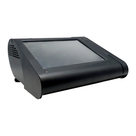
- Page 12 Chapter 1 Introduction POS-3120 SIDE VIEW Page: 1-6 ′ POS-3120 SERIES USER S MANUAL...
-
Page 13: System Specification
3 x DB-9, 1 x RJ45, +5V/ 12V selectable Universal Serial BUS Port: 4 x USB2.0 ports 1 x USB2.0 on side bezel LAN Function: 1 x 10/100/1000 Mbps Audio Function: 1 x 2W Speaker ′ Page: 1-7 POS-3120 SERIES USER S MANUAL... - Page 14 Read only, output through PS/2 KB interface MSR (Optional): JIS-I or II, ISO Tracker 1+2+3 (PS/2 KB Interface) Wireless LAN (Optional): Mini PCIe Wireless LAN Module (802.11b/g/n, 1T1R) Fingerprint (Optional): Embedded Fingerprint module (USB interface) Page: 1-8 ′ POS-3120 SERIES USER S MANUAL...
-
Page 15: Safety Precautions
Do not turn the system upside down. This may cause the hard drive to malfunction. c. Do not allow any objects to fall into this product. d. If water or other liquid spills into the product, unplug the power cord immediately. ′ Page: 1-9 POS-3120 SERIES USER S MANUAL... - Page 16 If heavy stains are present, moisten a cloth with diluted neutral washing agent or alcohol and then wipe thoroughly with a dry cloth. d. If dust is accumulated on the case surface, remove it by using a special vacuum cleaner for computers. Page: 1-10 ′ POS-3120 SERIES USER S MANUAL...
-
Page 17: Chapter 2 System Configuration
CHAPTER SYSTEM CONFIGURATION Helpful information that describes the jumper and connector settings, and component locations. Sections included: Jumper & Connector Quick Reference Table Component Locations Configuration and Jumper settings Connector Pin Assignments Page 2-1... -
Page 18: Jumper & Connector Quick Reference Table
Chapter 2 System Configuration 2-1. JUMPER & CONNECTOR QUICK REFERENCE TABLE Connector & Jumper Name Page COM1, COM3, COM4, COM2-1, COM Port & VGA Connector JVGACOM2 JP_COM1, JP_COM2, JP_COM3, COM Port RI and Voltage Selection 2-10 JP_COM4 MINI-DIN and USB Connector JPS2USB1, USB5, USB6 2-14 LAN &... -
Page 19: Component Locations
Chapter 2 System Configuration 2-2. COMPONENT LOCATIONS 72 71 COM3 PWR_IN1 POS-3120 Mainboard Front Connector, Jumper and Component locations Page: 2-3 ’ POS-3120 USER S MANUAL... - Page 20 Chapter 2 System Configuration M_PCIE1 POS-3120 Mainboard Rear Connector, Jumper and Component locations Page: 2-4 ’ POS-3120 USER S MANUAL...
-
Page 21: How To Set The Jumpers
Chapter 2 System Configuration 2-3. HOW TO SET THE JUMPERS You can configure your board by setting the jumpers. Jumper is consists of two or three metal pins with a plastic base mounted on the card, and by using a small plastic "cap", Also known as the jumper cap (with a metal contact inside), you are able to connect the pins. - Page 22 Chapter 2 System Configuration JUMPER DIAGRAMS JUMPER SETTINGS Page: 2-6 ’ POS-3120 USER S MANUAL...
-
Page 23: Com Port & Vga Connector
Chapter 2 System Configuration 2-4. COM PORT & VGA CONNECTOR There are four COM ports enhanced in this board namely: COM1, COM2, COM3 and COM4. Caution: When using a 72W power adaptor, do not set the voltage at “12V” for three COM ports or above; otherwise, the system may shut down due to power deficiency. - Page 24 Chapter 2 System Configuration COM4: COM4 Connector The pin assignments are as follows: ASSIGNMENT DCD4 COM4 RXD4 TXD4 DTR4 DSR4 RTS4 CTS4 RI / +5V / +12V selectable COM2-1: COM2 External Connector The pin assignments are as follows: ASSIGNMENT COM2-1 DCD1 RXD1 TXD1...
- Page 25 Chapter 2 System Configuration JVGACOM2: COM2 & VGA Connector The COM2 & VGA Connector assignments are as follows: ASSIGNMENT GREEN BLUE JVGACOM2 DDCA DATA HSYNC VSYNC DDCA CLK DCD1 RXD1 TXD1 DTR1 DSR1 RTS1 CTS1 RI / +5V / +12V selectable All COM port is selectable for RI, +5V or +12V.
- Page 26 Chapter 2 System Configuration 2-5. COM PORT RI & VOLTAGE SELECTION Caution: When using a 72W power adaptor, do not set the voltage at “12V” for three COM ports or above; otherwise, the system may shut down due to power deficiency. JP_COM1: COM1 RI &...
- Page 27 Chapter 2 System Configuration JP_COM2: COM2 RI & Voltage Selection The selections are as follows: JUMPER JUMPER SELECTION SETTINGS ILLUSTRATION VCC12 ***Manufacturing Default – RI Page: 2-11 ’ POS-3120 USER S MANUAL...
- Page 28 Chapter 2 System Configuration JP_COM3: COM3 RI & Voltage Selection The selections are as follows: JUMPER JUMPER SELECTION SETTINGS ILLUSTRATION VCC12 ***Manufacturing Default – RI Page: 2-12 ’ POS-3120 USER S MANUAL...
- Page 29 Chapter 2 System Configuration JP_COM4: COM4 RI & Voltage Selection The selections are as follows: JUMPER JUMPER SELECTION SETTINGS ILLUSTRATION VCC12 ***Manufacturing Default – RI Page: 2-13 ’ POS-3120 USER S MANUAL...
-
Page 30: Mini-Din And Usb Connector
Chapter 2 System Configuration 2-6. MINI-DIN AND USB CONNECTOR JPS2USB1: Two USB Ports Connector and MINI-DIM MINI-DIN connector can support keyboard, Y-cable, or PS/2 Mouse The pin assignments are as follows: ASSIGNMENT USB2+ USB2- VCC5 USB3+ USB3- VCC5 KDAT JPS2USB1 MDAT V5SB KCLK... -
Page 31: Lan & Usb Connector
Chapter 2 System Configuration USB6: Internal USB Ports Connector The pin assignments are as follows: ASSIGNMENT USB6- USB6+ VCC5 2-7. LAN & USB CONNECTOR JRJ45USB1: LAN & USB Connector The pin assignments are as follows: Green Orange ASSIGNMENT LAN1_MDIP0 LAN1_MDIN0 LAN1_MDIP1 LAN1_MDIN1 LAN1_MDIP2... -
Page 32: Cash Drawer Connector
Chapter 2 System Configuration 2-8. CASH DRAWER CONNECTOR DRW1, DRW2: Cash Drawer Connector The pin assignments are as follows: ASSIGNMENT Drawer Open Drawer Sense +12V DRW1 PROX-A3120 cash drawer control in GPIO port To Open Drawer1 (GPIO 7) Write "0"h to I/O space register "50C"h Bit 7 To Close Drawer1 Write "1"h to I/O space register "50C"h Bit 7 Detect Drawer1 Status... -
Page 33: Cash Drawer Power Selection
Chapter 2 System Configuration 2-9. CASH DRAWER POWER SELECTION JP14: Cash Drawer Power Selection The pin assignments are as follows: JUMPER JUMPER SELECTION SETTINGS ILLUSTRATION +12V +24V (default) *** Manufactory default – +24V Page: 2-17 ’ POS-3120 USER S MANUAL... -
Page 34: Power Led Connector
Chapter 2 System Configuration 2-10. POWER LED CONNECTOR LED_1: LED Connector The pin assignments are as follows: ASSIGNMENT VCC_PWR_LED 2-11. SMART FAN CONNECTOR FAN1: CPU Smart Fan Connector The pin assignments are as follows: ASSIGNMENT CPUFANIN CPUFANOUT 2-12. POWER CONNECTOR POWER1: Provide 12 Voltage Connector The pin assignments are as follows: ASSIGNMENT... -
Page 35: Reset Switch Connector
Chapter 2 System Configuration 2-13. RESET SWITCH CONNECTOR RST_SW1: Power Switch Connector The pin assignments are as follows: ASSIGNMENT RST_SW 2-14. POWER FOR THERMAL PRINTER CONNECTOR PRT_PWR1: Power for Thermal printer Connector The pin assignments are as follows: ASSIGNMENT VCC24SB VCC24SB 2-15. -
Page 36: Inverter Connector
Chapter 2 System Configuration 2-16. INVERTER CONNECTOR INV1: Inverter Connector The pin assignments are as follows: ASSIGNMENT +12V +12V LVDS_BKLTEN BRCTR INV2: Inverter Connector The pin assignments are as follows: ASSIGNMENT +12V LVDS_BKLTEN BRCTR Page: 2-20 ’ POS-3120 USER S MANUAL... -
Page 37: Msr/ Card Reader Connector
Chapter 2 System Configuration 2-17. MSR/ CARD READER CONNECTOR PS2: MSR/ Card Reader Connector The pin assignments are as follows: ASSIGNMENT KB_CLK (Output) KB_CLK_C (Input) KB_DATA_C (Input) KB_DATA (Output) 2-18. PRINTER CONNECTOR LPT1: LPT Connector. The assignments are as follows: ASSIGNMENT ASSIGNMENT STBJ... -
Page 38: Lvds Connector
Chapter 2 System Configuration 2-19. LVDS Connector LVDS1: LVDS Connector. The pin assignments are as follows: ASSIGNMENT ASSIGNMENT LVDS_VCC LVDS_YAP2 LVDS_VCC LVDS_YAM2 LVDS_YAP1 LVDS_CLKAP LVDS_YAM1 LVDS_CLKAM LVDS_YAP0 LVDS_YAM0 LVDS_VCC LVDS_VCC Page: 2-22 ’ POS-3120 USER S MANUAL... - Page 39 Chapter 2 System Configuration LVDS2: LVDS Connector. The pin assignments are as follows: ASSIGNMENT ASSIGNMENT LVDS_VCC CLKO+ CLKO- RINO2+ RINO2- RINO1+ RINO1- RINO0+ RINO0- LVDS_VCC LVDS_VCC Page: 2-23 ’ POS-3120 USER S MANUAL...
-
Page 40: Sata Connector
Chapter 2 System Configuration 2-20. SATA CONNECTOR SATA1: Serial ATA Connector The pin assignments are as follows: ASSIGNMENT 2-21. SATA POWER CONNECTOR JPWR_4P1: Serial ATA Connector The pin assignments are as follows: ASSIGNMENT VCC12 Page: 2-24 ’ POS-3120 USER S MANUAL... -
Page 41: Touch Panel Connector
Chapter 2 System Configuration 2-22. TOUCH PANEL CONNECTOR TOUCH1: Touch Panel Connector The pin assignments are as follows: ASSIGNMENT LR (Low Right) LL (Low Left) Probe UR (Up Right) UL (Up Left) 2-23. TOUCH PANEL SELECTION JP16: Touch Panel Selection The selections are as follows: JUMPER JUMPER... -
Page 42: Clear Cmos Data Selection
Chapter 2 System Configuration 2-24. CLEAR CMOS DATA SELECTION JP1: Clear CMOS Data Selection The selections are as follows: JUMPER JUMPER SELECTION SETTINGS ILLUSTRATION Clear CMOS Nornal *** Manufacturing Default – Normal To clear CMOS data, user must power-off the computer and set the jumper to “Clear CMOS”... -
Page 43: Compact Flash Connector
Chapter 2 System Configuration 2-25. COMPACT FLASH CONNECTOR CF1: Compact Flash Connector The pin assignments are as follows: ASSIGNMENT ASSIGNMENT CSJ1 CSJ3 SDIORDJ SDIOWRJ IRQ14 -CSEL RESETJ IORDJ ACKJ CF_LEDJ -PDIAG Page: 2-27 ’ POS-3120 USER S MANUAL... -
Page 44: Chapter 3 Software Utilities
CHAPTER SOFTWARE UTILITIES This chapter provides the detailed information users need to install driver utilities for the system. Sections included: ® Intel Chipset Software Installation Utility VGA Driver Utility LAN Driver Utility Sound Driver Utility Touch Screen Driver Utility Wireless Driver Utility (Optional) Page: 3-1... -
Page 45: Introduction
Chapter 3 Software Utilities 3-1. INTRODUCTION Enclosed with the POS-3120 Series package is our driver utilities, which comes in a CD ROM format. Refer to the following table for driver locations. Filename Purpose (Assume that CD ROM drive is D:) -
Page 46: Intel Chipset Software Installation Utility
Chapter 3 Software Utilities ® 3-2. INTEL C HIPSET SOFTWARE INSTALLATION UTILITY 3-2-1. Introduction ® The Intel Chipset Software Installation Utility installs to the target system the Windows* INF files that outline to the operating system how the chipset components will be configured. This is needed for the proper functioning of the following features: Core PCI and ISAPNP Services AGP Support... -
Page 47: Vga Driver Utility
Chapter 3 Software Utilities 3-3. VGA DRIVER UTILITY The VGA interface embedded with the POS-3120 series can support a wide range of display types. You can have dual displays via CRT and LVDS interfaces work simultaneously. 1. Win XP Series 2. -
Page 48: Lan Driver Utility
Chapter 3 Software Utilities 3-4. LAN DRIVER UTILITY The POS-3120 Series is enhanced with LAN function that can support various network adapters. Installation platform for the LAN driver is listed as follows: 1. Win XP Series 2. Win 7 Series For more details on Installation procedure, please refer to the Readme.txt file found on LAN Driver Utility. -
Page 49: Sound Driver Utility
Chapter 3 Software Utilities 3-5. SOUND DRIVER UTILITY The sound function enhanced in this system is fully compatible with Windows XP/ 7 series. Below, you will find the content of the Sound driver. 1. Win XP Series 2. Win 7 Series 3-5-1. -
Page 50: Touchscreen Driver Utility
Chapter 3 Software Utilities 3-6. TOUCHSCREEN DRIVER UTILITY The touchscreen driver utility can only be installed on a Windows platform (XP/ 7 series), and it should be installed right after the OS installation. 1. Win XP Series 2. Win 7 Series 3-6-1. -
Page 51: Wireless Driver Utility (Optional)
Chapter 3 Software Utilities 3-7. WIRELESS DRIVER UTILITY (OPTIONAL) The wireless driver utility can only be installed on a Windows platform (XP/ 7 series), and it should be installed right after the OS installation. 1. Win XP Series 2. Win 7 Series 3-7-1. -
Page 52: Introduction
CHAPTER BIOS SETUP This chapter shows how to configure the AMI BIOS settings. Sections included: Introduction Entering Setup Main Advanced Boot Security Chipset Exit Page: 4-1... - Page 53 Chapter 4 AMI BIOS Setup 4-1. INTRODUCTION This chapter will show you the function of the BIOS (Basic Input and Output System) in managing the features of your system. The A3120LF motherboard is equipped with the BIOS from AMI (American Megatrends Inc). The following pages describe how to use the BIOS for configure system hardware by BIOS Setup menu.
- Page 54 Chapter 4 AMI BIOS Setup 4-2 ENTERING SETUP When system powered on, BIOS will enter the Power-On Self Test (POST) routines and displays below message on the screen: American Megatrends www.ami.com AMI BIOS (C) 2009 American Megatrends, Inc. BIOS Date: 05/31/11 14:32:08 Ver: 08.00.16 Board BIOS Version: 31200P02 CPU : Intel (R) Atom (TM) CPU D525 @ 1.80GHz Speed : 1.80 GHz...
- Page 55 Chapter 4 AMI BIOS Setup BIOS SETUP UTILITY Main Advanced Boot Security Chipset Exit Use [ENTER], [TAB] System Overview or [SHIFT-TAB] to select a field. AMIBIOS Version :31200P02 Use [+] or [-] to Build Date :05/31/11 configure system Time. Processor Intel(R) Atom(TM) CPU D525 @1.80GHz Speed :1800MHz...
- Page 56 Chapter 4 AMI BIOS Setup 4-3. Main BIOS SETUP UTILITY Main Advanced Boot Security Chipset Exit Use [ENTER], [TAB] System Overview or [SHIFT-TAB] to select a field. AMIBIOS Version :31200P02 Use [+] or [-] to Build Date :05/31/11 configure system Time. Processor Intel(R) Atom(TM) CPU D525 @1.80GHz Speed...
- Page 57 Chapter 4 AMI BIOS Setup System Date This setting allows you to set the system date. The format is [Day Month/ Date/ Year]. User can directly key-in value or use <+> or <-> arrow keys to increase/decrease it. 4-4. Advanced BIOS SETUP UTILITY Main Advanced...
- Page 58 Chapter 4 AMI BIOS Setup 4-4.1. CPU Configuration BIOS SETUP UTILITY Main Advanced Boot Security Chipset Exit Enabled for Windows XP Configure advanced CPU settings and Linux4 (OS optimiz- Module Version: 3F. 1C ed for Hyper Threading Technology) and disab- Manufacturer :Intel led for other OS Intel(R) Atom(TM) CPU D525 @ 1.80GHz...
- Page 59 Chapter 4 AMI BIOS Setup 4-4.2. IDE Configuration BIOS SETUP UTILITY Main Advanced Boot Security Chipset Exit While entering setup, IDE Configuration BIOS auto detects the presence of IDE SATA1 [FUJITSU MHY20] devices. This displays CF Card [Not Detected] the status of auto detection of IDE devices.
- Page 60 Chapter 4 AMI BIOS Setup 4-4.2.1 SATA 1 and CF Card BIOS SETUP UTILITY Main Advanced Boot Security Chipset Exit Select the type SATA 1 of device connected to the system. Device :Hard Disk Vendor :FUJITSU MHY2040BH ESW Size :40.0GB LBA Mode : Supported Block Mode...
- Page 61 Chapter 4 AMI BIOS Setup Block (Multi-Sector Transfer) Any selection except Disabled determines the number of sectors transferred per block. PIO Mode Configure the type of PIO (Programmed Input/Output) mode 0-4 for IDE device. Mode 0 through 4 provides successively increased performance. DMA Mode Select the type of Ultra DMA mode on a hard drive.
- Page 62 Chapter 4 AMI BIOS Setup 4-4.3. SuperIO Configuration BIOS SETUP UTILITY Main Advanced Boot Security Chipset Exit Allows BIOS to set Configure Win627UHG Super IO Chipset WDTO function. Watchdog Function [Disabled] Serial Port1 Address [3F8] Serial Port1 IRQ [IRQ4] Serial Port2 Address [2F8] Serial Port2 IRQ [IRQ3]...
- Page 63 Chapter 4 AMI BIOS Setup Parallel Port Address Select IO address for parallel ports resource allocation. Parallel Port Mode Select the operation mode for parallel port. Parallel Port IRQ Select IRQ for parallel ports resource allocation. 4-4.4. Hardware Health Configuration BIOS SETUP UTILITY Main Advanced Boot Security Chipset...
- Page 64 Chapter 4 AMI BIOS Setup System Temperature / CPU Temperature Both section show System and CPU current temperature. CPUFAN Speed This item shows CPU fan speed. VCORE / 12V / 5V / 1.05V / VSB These items provide hardware health information. 4-4.5.
- Page 65 Chapter 4 AMI BIOS Setup Power Button Mode This setting controls shutdown action by pressing power button. The system will be shutdown immediately after pressing power button when set to “On/Off”. If set the power button mode to “Delay 4 seconds”, system will be shutdown after pressing and hold the power button over 4 seconds.
- Page 66 Chapter 4 AMI BIOS Setup 4-4.6.USB Configuration BIOS SETUP UTILITY Main Advanced Boot Security Chipset Exit Enables support for USB Configuration legacy USB. AUTO option disables Module Version – 2.24.5-14.4 legacy support if no USB devices are USB Devices Enabled : connected.
- Page 67 Chapter 4 AMI BIOS Setup 4-4.6.1 USB Mass Storage Device Configuration BIOS SETUP UTILITY Main Advanced Boot Security Chipset Exit USB Mass Storage Device Configuration If Auto, USB devices less than 530MB will be emulated as Floppy and remaining as Device #1 USB2.0 USB Flash Disk hard drive.
- Page 68 Chapter 4 AMI BIOS Setup 4-5. Boot BIOS SETUP UTILITY Main Advanced Boot Security Chipset Exit Configure Settings Boot Settings during System Boot. Boot Settings Configuration Boot Device Priority Hard Disk Drives PXE Support [Disabled] Select Screen Select Item Enter Go to Sub Screen General Help F10 Save and Exit ESC Exit...
- Page 69 Chapter 4 AMI BIOS Setup 4-5.1 Boot Settings Configuration BIOS SETUP UTILITY Main Advanced Boot Security Chipset Exit Allows BIOS to skip Boot Settings Configuration certain tests while booting. This will Quick Boot [Enabled] decrease the time Quiet Boot [Disabled] needed to boot the Parity Check [Disabled]...
- Page 70 Chapter 4 AMI BIOS Setup 4-5.2 Boot Device Priority BIOS SETUP UTILITY Main Advanced Boot Security Chipset Exit Specifies the boot Boot Device Priority sequence from the available devices. 1st Boot Device [USB:USB2.0 USB Fla] A device enclosed in parenthesis has been disabled in the corresponding type menu.
- Page 71 Chapter 4 AMI BIOS Setup 4-5.3 Hard Disk Drives BIOS SETUP UTILITY Main Advanced Boot Security Chipset Exit Specifies the boot Hard Disk Drives sequence from the available devices. 1st Drive [USB:USB2.0 USB Fla] 2nd Drive [SATA: PM-FUJITSU MH] Select Screen Select Item Change Option General Help...
- Page 72 Chapter 4 AMI BIOS Setup 4-6. Security BIOS SETUP UTILITY Main Advanced Boot Security Chipset Exit Install or Change the Security Settings password. Supervisor Password :Not Installed User Password :Not Installed Change Supervisor Password Change User Password Clear User Password Select Screen Select Item Enter Change...
- Page 73 Chapter 4 AMI BIOS Setup 4.7 Chipset BIOS SETUP UTILITY Main Advanced Boot Security Chipset Exit Configure North Bridge Advanced Chipset Settings features. WARNING: Setting wrong values in below sections may cause system to malfunction. North Bridge Configuration South Bridge Configuration Select Screen Select Item Enter Go to Sub Screen...
- Page 74 Chapter 4 AMI BIOS Setup 4-7.1 North Bridge Chipset Configuration BIOS SETUP UTILITY Main Advanced Boot Security Chipset Exit North Bridge Chipset Configuration Video Function Configuration Select Screen Select Item Change Option General Help F10 Save and Exit ESC Exit v02.68 (c)Copyright 1985-2009 American Megatrends, Inc.
- Page 75 Chapter 4 AMI BIOS Setup 4-7.1.1 Video Function Configuration BIOS SETUP UTILITY Main Advanced Boot Security Chipset Exit Options Video Function Configuration DVMT Mode Select [DVMT Mode] Fixed Mode DVMT/FIXED Memory [256MB] DVMT Mode Boot Display Device [CRT + LVDS] Flat Panel Type [1024x768] Select Screen...
- Page 76 Chapter 4 AMI BIOS Setup Boot Display Device Choose the default boot display device by user requirement such as [CRT], [LVDS] and [CRT+LVDS] Flat Panel Type Select the resolution for the connected LVDS panel such as [800x600] and [1024x768]. 4-7.2 South Bridge Configuration BIOS SETUP UTILITY Main Advanced Boot Security Chipset...
- Page 77 Chapter 4 AMI BIOS Setup USB 2.0 Controller Enable the USB 2.0 Controller. HDA Controller Enable or disable the onboard High-definition Audio controller. 4.8 Exit BIOS SETUP UTILITY Main Advanced Boot Security Chipset Exit Exit system setup Exit Options after saving the changes.
- Page 78 Chapter 4 AMI BIOS Setup Discard Changes and Exit Abandon all changes and exit the BIOS setup screen. User can also press the [ESC] key for this operation. Discard Changes Discard all changes done so far to the setup items. User can press the [F7] key for this operation.
-
Page 79: Exploded Diagram For Pos-3120 Msr Assembly
APPENDIX SYSTEM ASSEMBLY This appendix contains exploded diagrams and part numbers of the POS-3120 system. Sections included: Exploded Diagram for 2 Inch Thermal Printer Assembly Exploded Diagram for 3 Inch Thermal Printer Assembly Exploded Diagram for Printer Paper Holder Assembly ... -
Page 80: Exploded Diagram For 2 Inch Thermal Printer Assembly
Appendix A System Assembly EXPLODED DIAGRAM FOR 2 INCH THERMAL PRINTER ASSEMBLY Page: A-2 POS-3120 USER S MANUAL... - Page 81 Appendix A System Assembly Page: A-3 POS-3120 USER S MANUAL...
- Page 82 Appendix A System Assembly Page: A-4 POS-3120 USER S MANUAL...
- Page 83 Appendix A System Assembly Page: A-5 POS-3120 USER S MANUAL...
-
Page 84: Exploded Diagram For 3 Inch Thermal Printer Assembly
Appendix A System Assembly EXPLODED DIAGRAM FOR 3 INCH THERMAL PRINTER ASSEMBLY Page: A-6 POS-3120 USER S MANUAL... - Page 85 Appendix A System Assembly Page: A-7 POS-3120 USER S MANUAL...
- Page 86 Appendix A System Assembly Page: A-8 POS-3120 USER S MANUAL...
-
Page 87: Exploded Diagram For Printer Paper Holder Assembly
Appendix A System Assembly EXPLODED DIAGRAM FOR PRINTER PAPER HOLDER ASSEMBLY Page: A-9 POS-3120 USER S MANUAL... -
Page 88: Exploded Diagram For Fan Assembly
Appendix A System Assembly EXPLODED DIAGRAM FOR FAN ASSEMBLY Page: A-10 POS-3120 USER S MANUAL... - Page 89 Appendix A System Assembly Page: A-11 POS-3120 USER S MANUAL...
-
Page 90: Exploded Diagram For Empty Top Case Assembly
Appendix A System Assembly EXPLODED DIAGRAM FOR EMPTY TOP CASE ASSEMBLY Page: A-12 POS-3120 USER S MANUAL... - Page 91 Appendix A System Assembly Page: A-13 POS-3120 USER S MANUAL...
-
Page 92: Exploded Diagram For Fingerprint Module
Appendix A System Assembly EXPLODED DIAGRAM FOR FINGERPRINT MODULE Page: A-14 POS-3120 USER S MANUAL... - Page 93 Appendix A System Assembly Page: A-15 POS-3120 USER S MANUAL...
-
Page 94: Exploded Diagram For Pos-3120 Hard Disk Drive Assembly
Appendix A System Assembly EXPLODED DIAGRAM FOR POS-3120 HARD DISK DRIVE ASSEMBLY Page: A-16 POS-3120 USER S MANUAL... - Page 95 Appendix A System Assembly Page: A-17 POS-3120 USER S MANUAL...
- Page 96 Appendix A System Assembly Page: A-18 POS-3120 USER S MANUAL...
-
Page 97: Exploded Diagram For I-Button Assembly
Appendix A System Assembly EXPLODED DIAGRAM FOR I-BUTTON ASSEMBLY Page: A-19 POS-3120 USER S MANUAL... - Page 98 Appendix A System Assembly Page: A-20 POS-3120 USER S MANUAL...
-
Page 99: Exploded Diagram For Pos-3120 Cpt Lcd Assembly
Appendix A System Assembly EXPLODED DIAGRAM FOR POS-3120 CPT LCD ASSEMBLY Page: A-21 POS-3120 USER S MANUAL... - Page 100 Appendix A System Assembly Page: A-22 POS-3120 USER S MANUAL...
-
Page 101: Exploded Diagram For Pos-3120 Data Image Lcd Assembly
Appendix A System Assembly EXPLODED DIAGRAM FOR POS-3120 DATA IMAGE LCD ASSEMBLY Page: A-23 POS-3120 USER S MANUAL... - Page 102 Appendix A System Assembly Page: A-24 POS-3120 USER S MANUAL...
-
Page 103: Exploded Diagram For Pos-3120 Mini-Pcie Installation
Appendix A System Assembly EXPLODED DIAGRAM FOR POS-3120 MINI-PCIE INSTALLATION Page: A-25 POS-3120 USER S MANUAL... - Page 104 Appendix A System Assembly Page: A-26 POS-3120 USER S MANUAL...
-
Page 105: Exploded Diagram For Pos-3120 Motherboard
Appendix A System Assembly EXPLODED DIAGRAM FOR POS-3120 MOTHERBOARD Page: A-27 POS-3120 USER S MANUAL... - Page 106 Appendix A System Assembly Page: A-28 POS-3120 USER S MANUAL...
- Page 107 Appendix A System Assembly Page: A-29 POS-3120 USER S MANUAL...
- Page 108 Appendix A System Assembly Page: A-30 POS-3120 USER S MANUAL...
- Page 109 Appendix A System Assembly EXPLODED DIAGRAM FOR POS-3120 MSR ASSEMBLY Page: A-31 POS-3120 USER S MANUAL...
-
Page 110: Exploded Diagram For Pos-3120 Msr Module
Appendix A System Assembly EXPLODED DIAGRAM FOR POS-3120 MSR MODULE Page: A-32 POS-3120 USER S MANUAL... - Page 111 Appendix A System Assembly Page: A-33 POS-3120 USER S MANUAL...
-
Page 112: Exploded Diagram For Pos-3120 Printer Assembly
Appendix A System Assembly EXPLODED DIAGRAM FOR POS-3120 PRINTER ASSEMBLY Page: A-34 POS-3120 USER S MANUAL... - Page 113 Appendix A System Assembly Page: A-35 POS-3120 USER S MANUAL...
-
Page 114: Exploded Diagram For Pos-3120 Top Cover Assembly
Appendix A System Assembly EXPLODED DIAGRAM FOR POS-3120 TOP COVER ASSEMBLY Page: A-36 POS-3120 USER S MANUAL... -
Page 115: Exploded Diagram For Vfd Module Assembly
Appendix A System Assembly EXPLODED DIAGRAM FOR VFD MODULE ASSEMBLY Page: A-37 POS-3120 USER S MANUAL... - Page 116 Appendix A System Assembly Page: A-38 POS-3120 USER S MANUAL...
- Page 117 APPENDIX TECHNICAL SUMMARY This appendix will give you a brief introduction of the allocation maps for the system resources. Sections included: Block Diagram Interrupt Map DMA Channels Map I / O Map Watchdog Timer Configuration Flash BIOS Update Page: B-1...
-
Page 118: Appendix B Technical Summary
Appendix B Technical Summary BLOCK DIAGRAM Page: B-2 ′ POS-3120 SERIES USER S MANUAL... -
Page 119: Interrupt Map
Intel(R) ICH8 Family PCI Express Root Port 1 - 283F Intel(R) ICH8 Family PCI Express Root Port 6 - 2849 Intel(R) ICH8 Family USB Universal Host Controller – 2830 Intel(R) ICH8 Family USB2 Enhanced Host Controller - 2836 ′ Page: B-3 POS-3120 SERIES USER S MANUAL... -
Page 120: Dma Channels Map
Appendix B Technical Summary DMA CHANNELS MAP DMA Channel Assignment Direct memory access controller Page: B-4 ′ POS-3120 SERIES USER S MANUAL... -
Page 121: I/O Map
Motherboard resources 0x000000F0-0x000000FF Numeric data processor 0x000001F0-0x000001F7 Primary IDE Channel 0x00000274-0x00000277 ISAPNP Read Data Port 0x00000279-0x00000279 ISAPNP Read Data Port 0x000002E8-0x000002EF Communications Port (COM4) 0x000002F8-0x000002FF Communications Port (COM2) 0x00000378-0x0000037F Printer Port (LPT1) ′ Page: B-5 POS-3120 SERIES USER S MANUAL... - Page 122 Intel(R) ICH8M 3 port Serial ATA Storage Controller - 2828 0x0000E000-0x0000FFFF Intel(R) ICH8 Family PCI Express Root Port 6 - 2849 0x0000E800-0x0000E8FF Realtek PCIe GBE Family Controller 0x0000FFA0-0x0000FFAF Intel(R) ICH8M Ultra ATA Storage Controllers - 2850 Page: B-6 ′ POS-3120 SERIES USER S MANUAL...
-
Page 123: Watchdog Timer Configuration
(3) Exit the extended function mode To exit the Extended Function Mode, writing 0xAA to the EFER is required. Once SuperIO exits the Extended Function Mode, it goes back to the normal running mode. ′ Page: B-7 POS-3120 SERIES USER S MANUAL... - Page 124 ;------ Logic device activation for watch dog timer ------------------------------------------ 030h ;------ Set second as counting unit -------------------------------------------------------------- 0F5h not 08h ;------ Set timeout interval as 30seconds and start counting --------------------------------- 0F6h ;------ Exit the extended function mode -------------------------------------------------------- 0AAh Page: B-8 ′ POS-3120 SERIES USER S MANUAL...
- Page 125 (4) Select [Boot] menu. (5) Select [Boot Devices Priority] sub-menu, set the USB bootable device to be the 1 boot device. (6) Press <F10> key to save configuration and exit the BIOS setup menu. ′ Page: B-9 POS-3120 SERIES USER S MANUAL...
- Page 126 User can type “AFUDOS/?” to see all the definition of each control options. The recommended options for BIOS ROM update include following parameters: Program main BIOS image. /B: Program Boot Block. /N: Program NVRAM. /C: Destroy CMOS checksum /X: Don’t check ROM ID. Page: B-10 ′ POS-3120 SERIES USER S MANUAL...
- Page 127 After BIOS update procedures is complete, the messages should be like the figure shown below. User can restart the system and boot up with new BIOS now. ′ Page: B-11 POS-3120 SERIES USER S MANUAL...
- Page 128 USER’S MANUAL POS-3120 Series Mini POS System Powered by ® ® Intel Atom Platform POS-3120 Series M5...
- Page 129 Preface POS-3120 Series POS System With LCD / Touchscreen PREFACE COPYRIGHT NOTICE This user’s manual is meant to assist users in installing and setting up the system. The information contained in this document is subject to change without any notice.
- Page 130 Preface FCC NOTICE This equipment has been tested and found to comply with the limits for a Class A digital device, pursuant to part 15 of the FCC Rules. These limits are designed to provide reasonable protection against harmful interference when the equipment is operated in a commercial environment.
- Page 131 Contents TABLE OF CONTENTS CHAPTER 1 INTRODUCTION About This Manual ............POS System Illustration ..........System Specification ............. Safety Precautions ............CHAPTER 2 SYSTEM CONFIGURATION Jumper & Connector Quick Reference Table ....Component Locations ............ How to Set the Jumpers ..........COM Port &...
- Page 132 Contents CHAPTER 3 SOFTWARE UTILITIES Introduction …............... ® Intel Chipset Software Installation Utility …....VGA Driver Utility …………………………….…….. LAN Driver Utility …............ Sound Driver Utility …..........Touch Screen Driver Utility ………………………….. Wireless Driver Utility (Optional) ……………………. CHAPTER 4 AMI BIOS SETUP Introduction …...............
- Page 133 Contents Exploded Diagram for POS-3120 MSR Assembly …..……… A-31 Exploded Diagram for POS-3120 MSR Module ……………. A-32 Exploded Diagram for POS-3120 Printer Assembly ………… A-34 Exploded Diagram for POS-3120 Top Cover Assembly ….… A-36 Exploded Diagram for VFD Module Assembly ……………... A-37 APPENDIX B TECHNICAL SUMMARY Block Diagram .................
-
Page 134: Chapter 1 Introduction
CHAPTER INTRODUCTION This chapter gives you the information for the POS-3120. It also outlines the system specifications. Sections included: About This Manual POS System Illustration System Specifications Safety Precautions Experienced users can jump to chapter 2 on page 2-1 for a quick start. Page:1-1... -
Page 135: About This Manual
Chapter 1 Introduction 1-1. ABOUT THIS MANUAL Thank you for purchasing our POS-3120 Series System. The POS-3120 is an updated system designed to be comparable with the highest performance of IBM AT personal computers. The POS-3120 provides faster processing speed, greater expandability and can handle more tasks than before. -
Page 136: Pos System Illustration
Chapter 1 Introduction 1-2. POS SYSTEM ILLUSTRATION POS-3120 i-Button Type ′ Page: 1-3 POS-3120 SERIES USER S MANUAL... - Page 137 Chapter 1 Introduction POS-3120 Finger Printer Type Page: 1-4 ′ POS-3120 SERIES USER S MANUAL...
- Page 138 Chapter 1 Introduction POS-3120 Empty Type ′ Page: 1-5 POS-3120 SERIES USER S MANUAL...
- Page 139 Chapter 1 Introduction POS-3120 SIDE VIEW Page: 1-6 ′ POS-3120 SERIES USER S MANUAL...
-
Page 140: System Specification
3 x DB-9, 1 x RJ45, +5V/ 12V selectable Universal Serial BUS Port: 4 x USB2.0 ports 1 x USB2.0 on side bezel LAN Function: 1 x 10/100/1000 Mbps Audio Function: 1 x 2W Speaker ′ Page: 1-7 POS-3120 SERIES USER S MANUAL... - Page 141 Read only, output through PS/2 KB interface MSR (Optional): JIS-I or II, ISO Tracker 1+2+3 (PS/2 KB Interface) Wireless LAN (Optional): Mini PCIe Wireless LAN Module (802.11b/g/n, 1T1R) Fingerprint (Optional): Embedded Fingerprint module (USB interface) Page: 1-8 ′ POS-3120 SERIES USER S MANUAL...
-
Page 142: Safety Precautions
Do not turn the system upside down. This may cause the hard drive to malfunction. c. Do not allow any objects to fall into this product. d. If water or other liquid spills into the product, unplug the power cord immediately. ′ Page: 1-9 POS-3120 SERIES USER S MANUAL... - Page 143 If heavy stains are present, moisten a cloth with diluted neutral washing agent or alcohol and then wipe thoroughly with a dry cloth. d. If dust is accumulated on the case surface, remove it by using a special vacuum cleaner for computers. Page: 1-10 ′ POS-3120 SERIES USER S MANUAL...
-
Page 144: Chapter 2 System Configuration
CHAPTER SYSTEM CONFIGURATION Helpful information that describes the jumper and connector settings, and component locations. Sections included: Jumper & Connector Quick Reference Table Component Locations Configuration and Jumper settings Connector Pin Assignments Page 2-1... -
Page 145: Jumper & Connector Quick Reference Table
Chapter 2 System Configuration 2-1. JUMPER & CONNECTOR QUICK REFERENCE TABLE Connector & Jumper Name Page COM1, COM3, COM4, COM2-1, COM Port & VGA Connector JVGACOM2 JP_COM1, JP_COM2, JP_COM3, COM Port RI and Voltage Selection 2-10 JP_COM4 MINI-DIN and USB Connector JPS2USB1, USB5, USB6 2-14 LAN &... - Page 146 Chapter 2 System Configuration 2-2. COMPONENT LOCATIONS M/B: PB-3120RB RST_SW1 SPK1 INV2 USB6 LVDS1 LED_1 LVDS2 JP13 TOUCH1 JINVDRV1 JP15 INV1 JP18 BAT1 DIMM2 LPT1 Intel ICH8M Atom D525 72 71 POWER1 JPWR_4P1 DIMM1 USB4-1 SATA1 JP12 FAN1 COM2-1 COM4 JP10 USB5 PRT_PWR1...
- Page 147 Chapter 2 System Configuration M_PCIE1 POS-3120 Mainboard Rear Connector, Jumper and Component locations Page: 2-4 ’ POS-3120 USER S MANUAL...
-
Page 148: How To Set The Jumpers
Chapter 2 System Configuration 2-3. HOW TO SET THE JUMPERS You can configure your board by setting the jumpers. Jumper is consists of two or three metal pins with a plastic base mounted on the card, and by using a small plastic "cap", Also known as the jumper cap (with a metal contact inside), you are able to connect the pins. - Page 149 Chapter 2 System Configuration JUMPER DIAGRAMS JUMPER SETTINGS Page: 2-6 ’ POS-3120 USER S MANUAL...
-
Page 150: Com Port & Vga Connector
Chapter 2 System Configuration 2-4. COM PORT & VGA CONNECTOR There are four COM ports enhanced in this board namely: COM1, COM2, COM3 and COM4. Caution: When using a 72W power adaptor, do not set the voltage at “12V” for three COM ports or above; otherwise, the system may shut down due to power deficiency. - Page 151 Chapter 2 System Configuration COM4: COM4 Connector The pin assignments are as follows: ASSIGNMENT DCD4 COM4 RXD4 TXD4 DTR4 DSR4 RTS4 CTS4 RI / +5V / +12V selectable COM2-1: COM2 External Connector The pin assignments are as follows: ASSIGNMENT COM2-1 DCD1 RXD1 TXD1...
- Page 152 Chapter 2 System Configuration JVGACOM2: COM2 & VGA Connector The COM2 & VGA Connector assignments are as follows: ASSIGNMENT GREEN BLUE JVGACOM2 DDCA DATA HSYNC VSYNC DDCA CLK DCD1 RXD1 TXD1 DTR1 DSR1 RTS1 CTS1 RI / +5V / +12V selectable All COM port is selectable for RI, +5V or +12V.
- Page 153 Chapter 2 System Configuration 2-5. COM PORT RI & VOLTAGE SELECTION Caution: When using a 72W power adaptor, do not set the voltage at “12V” for three COM ports or above; otherwise, the system may shut down due to power deficiency. JP_COM1: COM1 RI &...
- Page 154 Chapter 2 System Configuration JP_COM2: COM2 RI & Voltage Selection The selections are as follows: JUMPER JUMPER SELECTION SETTINGS ILLUSTRATION VCC12 ***Manufacturing Default – RI Page: 2-11 ’ POS-3120 USER S MANUAL...
- Page 155 Chapter 2 System Configuration JP_COM3: COM3 RI & Voltage Selection The selections are as follows: JUMPER JUMPER SELECTION SETTINGS ILLUSTRATION VCC12 ***Manufacturing Default – RI Page: 2-12 ’ POS-3120 USER S MANUAL...
- Page 156 Chapter 2 System Configuration JP_COM4: COM4 RI & Voltage Selection The selections are as follows: JUMPER JUMPER SELECTION SETTINGS ILLUSTRATION VCC12 ***Manufacturing Default – RI Page: 2-13 ’ POS-3120 USER S MANUAL...
-
Page 157: Mini-Din And Usb Connector
Chapter 2 System Configuration 2-6. MINI-DIN AND USB CONNECTOR JPS2USB1: Two USB Ports Connector and MINI-DIM MINI-DIN connector can support keyboard, Y-cable, or PS/2 Mouse The pin assignments are as follows: ASSIGNMENT USB2+ USB2- VCC5 USB3+ USB3- VCC5 KDAT MDAT V5SB KCLK MCLK... -
Page 158: Lan & Usb Connector
Chapter 2 System Configuration USB6: Internal USB Ports Connector The pin assignments are as follows: ASSIGNMENT USB6- USB6+ VCC5 2-7. LAN & USB CONNECTOR JRJ45USB1: LAN & USB Connector The pin assignments are as follows: Green Orange ASSIGNMENT LAN1_MDIP0 LAN1_MDIN0 LAN1_MDIP1 LAN1_MDIN1 LAN1_MDIP2... -
Page 159: Cash Drawer Connector
Chapter 2 System Configuration 2-8. CASH DRAWER CONNECTOR DRW1, DRW2: Cash Drawer Connector The pin assignments are as follows: ASSIGNMENT Drawer Open Drawer Sense +12V DRW1 PROX-A3120 cash drawer control in GPIO port To Open Drawer1 (GPIO 7) Write "0"h to I/O space register "50C"h Bit 7 To Close Drawer1 Write "1"h to I/O space register "50C"h Bit 7 Detect Drawer1 Status... -
Page 160: Cash Drawer Power Selection
Chapter 2 System Configuration 2-9. CASH DRAWER POWER SELECTION JP14: Cash Drawer Power Selection The pin assignments are as follows: JUMPER JUMPER SELECTION SETTINGS ILLUSTRATION +12V +24V (default) *** Manufactory default – +24V Page: 2-17 ’ POS-3120 USER S MANUAL... -
Page 161: Power Led Connector
Chapter 2 System Configuration 2-10. POWER LED CONNECTOR LED_1: LED Connector The pin assignments are as follows: ASSIGNMENT VCC_PWR_LED 2-11. SMART FAN CONNECTOR FAN1: CPU Smart Fan Connector The pin assignments are as follows: ASSIGNMENT CPUFANIN CPUFANOUT 2-12. POWER CONNECTOR POWER1: Provide 12 Voltage Connector The pin assignments are as follows: ASSIGNMENT... -
Page 162: Reset Switch Connector
Chapter 2 System Configuration 2-13. RESET SWITCH CONNECTOR RST_SW1: Power Switch Connector The pin assignments are as follows: ASSIGNMENT RST_SW 2-14. POWER FOR THERMAL PRINTER CONNECTOR PRT_PWR1: Power for Thermal printer Connector The pin assignments are as follows: ASSIGNMENT VCC24SB VCC24SB 2-15. -
Page 163: Inverter Connector
Chapter 2 System Configuration 2-16. INVERTER CONNECTOR INV1: Inverter Connector The pin assignments are as follows: ASSIGNMENT +12V +12V LVDS_BKLTEN BRCTR INV2: Inverter Connector The pin assignments are as follows: ASSIGNMENT +12V LVDS_BKLTEN BRCTR Page: 2-20 ’ POS-3120 USER S MANUAL... -
Page 164: Msr/ Card Reader Connector
Chapter 2 System Configuration 2-17. MSR/ CARD READER CONNECTOR PS2: MSR/ Card Reader Connector The pin assignments are as follows: ASSIGNMENT KB_CLK (Output) KB_CLK_C (Input) KB_DATA_C (Input) KB_DATA (Output) 2-18. PRINTER CONNECTOR LPT1: LPT Connector. The assignments are as follows: ASSIGNMENT ASSIGNMENT STBJ... -
Page 165: Lvds Connector
Chapter 2 System Configuration 2-19. LVDS Connector LVDS1: LVDS Connector. The pin assignments are as follows: ASSIGNMENT ASSIGNMENT LVDS_VCC LVDS_YAP2 LVDS_VCC LVDS_YAM2 LVDS_YAP1 LVDS_CLKAP LVDS_YAM1 LVDS_CLKAM LVDS_YAP0 LVDS_YAM0 LVDS_VCC LVDS_VCC Page: 2-22 ’ POS-3120 USER S MANUAL... - Page 166 Chapter 2 System Configuration LVDS2: LVDS Connector. The pin assignments are as follows: ASSIGNMENT ASSIGNMENT LVDS_VCC CLKO+ CLKO- RINO2+ RINO2- RINO1+ RINO1- RINO0+ RINO0- LVDS_VCC LVDS_VCC Page: 2-23 ’ POS-3120 USER S MANUAL...
-
Page 167: Sata Connector
Chapter 2 System Configuration 2-20. SATA CONNECTOR SATA1: Serial ATA Connector The pin assignments are as follows: ASSIGNMENT 2-21. SATA POWER CONNECTOR JPWR_4P1: Serial ATA Connector The pin assignments are as follows: ASSIGNMENT VCC12 2-22. TOUCH PANEL CONNECTOR TOUCH1: Touch Panel Connector The pin assignments are as follows: ASSIGNMENT LR (Low Right) -
Page 168: Clear Cmos Data Selection
Chapter 2 System Configuration 2-23. CLEAR CMOS DATA SELECTION JP1: Clear CMOS Data Selection The selections are as follows: JUMPER JUMPER SELECTION SETTINGS ILLUSTRATION Clear CMOS Nornal *** Manufacturing Default – Normal To clear CMOS data, user must power-off the computer and set the jumper to “Clear CMOS”... -
Page 169: Compact Flash Connector
Chapter 2 System Configuration 2-24. COMPACT FLASH CONNECTOR CF1: Compact Flash Connector The pin assignments are as follows: ASSIGNMENT ASSIGNMENT CSJ1 CSJ3 SDIORDJ SDIOWRJ IRQ14 -CSEL RESETJ IORDJ ACKJ CF_LEDJ -PDIAG Page: 2-26 ’ POS-3120 USER S MANUAL... -
Page 170: Backlight Type Selection
Chapter 2 System Configuration 2-25. LED BACKLIGHT POWER CONNECTOR JINVDRV1: LED Backlight Power Connector The pin assignments are as follows: ASSIGNMENT JINVDRV1 2-26. BACKLIGHT TYPE SELECTION JP18: Backlight Type Selection The selections are as follows: JUMPER JUMPER SELECTION SETTINGS ILLUSTRATION JP18 CCFL JP18... -
Page 171: Chapter 3 Software Utilities
CHAPTER SOFTWARE UTILITIES This chapter provides the detailed information users need to install driver utilities for the system. Sections included: ® Intel Chipset Software Installation Utility VGA Driver Utility LAN Driver Utility Sound Driver Utility Touch Screen Driver Utility Wireless Driver Utility (Optional) Page: 3-1... -
Page 172: Introduction
Chapter 3 Software Utilities 3-1. INTRODUCTION Enclosed with the POS-3120 Series package is our driver utilities, which comes in a CD ROM format. Refer to the following table for driver locations. Filename Purpose (Assume that CD ROM drive is D:) -
Page 173: Intel Chipset Software Installation Utility
Chapter 3 Software Utilities ® 3-2. INTEL C HIPSET SOFTWARE INSTALLATION UTILITY 3-2-1. Introduction ® The Intel Chipset Software Installation Utility installs to the target system the Windows* INF files that outline to the operating system how the chipset components will be configured. This is needed for the proper functioning of the following features: Core PCI and ISAPNP Services AGP Support... -
Page 174: Vga Driver Utility
Chapter 3 Software Utilities 3-3. VGA DRIVER UTILITY The VGA interface embedded with the POS-3120 series can support a wide range of display types. You can have dual displays via CRT and LVDS interfaces work simultaneously. 1. Win XP Series 2. -
Page 175: Lan Driver Utility
Chapter 3 Software Utilities 3-4. LAN DRIVER UTILITY The POS-3120 Series is enhanced with LAN function that can support various network adapters. Installation platform for the LAN driver is listed as follows: 1. Win XP Series 2. Win 7 Series For more details on Installation procedure, please refer to the Readme.txt file found on LAN Driver Utility. -
Page 176: Sound Driver Utility
Chapter 3 Software Utilities 3-5. SOUND DRIVER UTILITY The sound function enhanced in this system is fully compatible with Windows XP/ 7 series. Below, you will find the content of the Sound driver. 1. Win XP Series 2. Win 7 Series 3-5-1. -
Page 177: Touchscreen Driver Utility
Chapter 3 Software Utilities 3-6. TOUCHSCREEN DRIVER UTILITY The touchscreen driver utility can only be installed on a Windows platform (XP/ 7 series), and it should be installed right after the OS installation. 1. Win XP Series 2. Win 7 Series 3-6-1. -
Page 178: Wireless Driver Utility (Optional)
Chapter 3 Software Utilities 3-7. WIRELESS DRIVER UTILITY (OPTIONAL) The wireless driver utility can only be installed on a Windows platform (XP/ 7 series), and it should be installed right after the OS installation. 1. Win XP Series 2. Win 7 Series 3-7-1. -
Page 179: Introduction
CHAPTER BIOS SETUP This chapter shows how to configure the AMI BIOS settings. Sections included: Introduction Entering Setup Main Advanced Boot Security Chipset Exit Page: 4-1... - Page 180 Chapter 4 AMI BIOS Setup 4-1. INTRODUCTION This chapter will show you the function of the BIOS (Basic Input and Output System) in managing the features of your system. The A3120LF motherboard is equipped with the BIOS from AMI (American Megatrends Inc). The following pages describe how to use the BIOS for configure system hardware by BIOS Setup menu.
- Page 181 Chapter 4 AMI BIOS Setup 4-2 ENTERING SETUP When system powered on, BIOS will enter the Power-On Self Test (POST) routines and displays below message on the screen: American Megatrends www.ami.com AMI BIOS (C) 2009 American Megatrends, Inc. BIOS Date: 05/31/11 14:32:08 Ver: 08.00.16 Board BIOS Version: 31200P02 CPU : Intel (R) Atom (TM) CPU D525 @ 1.80GHz Speed : 1.80 GHz...
- Page 182 Chapter 4 AMI BIOS Setup BIOS SETUP UTILITY Main Advanced Boot Security Chipset Exit Use [ENTER], [TAB] System Overview or [SHIFT-TAB] to select a field. AMIBIOS Version :31200P02 Use [+] or [-] to Build Date :05/31/11 configure system Time. Processor Intel(R) Atom(TM) CPU D525 @1.80GHz Speed :1800MHz...
- Page 183 Chapter 4 AMI BIOS Setup 4-3. Main BIOS SETUP UTILITY Main Advanced Boot Security Chipset Exit Use [ENTER], [TAB] System Overview or [SHIFT-TAB] to select a field. AMIBIOS Version :31200P02 Use [+] or [-] to Build Date :05/31/11 configure system Time. Processor Intel(R) Atom(TM) CPU D525 @1.80GHz Speed...
- Page 184 Chapter 4 AMI BIOS Setup System Date This setting allows you to set the system date. The format is [Day Month/ Date/ Year]. User can directly key-in value or use <+> or <-> arrow keys to increase/decrease it. 4-4. Advanced BIOS SETUP UTILITY Main Advanced...
- Page 185 Chapter 4 AMI BIOS Setup 4-4.1. CPU Configuration BIOS SETUP UTILITY Main Advanced Boot Security Chipset Exit Enabled for Windows XP Configure advanced CPU settings and Linux4 (OS optimiz- Module Version: 3F. 1C ed for Hyper Threading Technology) and disab- Manufacturer :Intel led for other OS Intel(R) Atom(TM) CPU D525 @ 1.80GHz...
- Page 186 Chapter 4 AMI BIOS Setup 4-4.2. IDE Configuration BIOS SETUP UTILITY Main Advanced Boot Security Chipset Exit While entering setup, IDE Configuration BIOS auto detects the presence of IDE SATA1 [FUJITSU MHY20] devices. This displays CF Card [Not Detected] the status of auto detection of IDE devices.
- Page 187 Chapter 4 AMI BIOS Setup 4-4.2.1 SATA 1 and CF Card BIOS SETUP UTILITY Main Advanced Boot Security Chipset Exit Select the type SATA 1 of device connected to the system. Device :Hard Disk Vendor :FUJITSU MHY2040BH ESW Size :40.0GB LBA Mode : Supported Block Mode...
- Page 188 Chapter 4 AMI BIOS Setup Block (Multi-Sector Transfer) Any selection except Disabled determines the number of sectors transferred per block. PIO Mode Configure the type of PIO (Programmed Input/Output) mode 0-4 for IDE device. Mode 0 through 4 provides successively increased performance. DMA Mode Select the type of Ultra DMA mode on a hard drive.
- Page 189 Chapter 4 AMI BIOS Setup 4-4.3. SuperIO Configuration BIOS SETUP UTILITY Main Advanced Boot Security Chipset Exit Allows BIOS to set Configure Win627UHG Super IO Chipset WDTO function. Watchdog Function [Disabled] Serial Port1 Address [3F8] Serial Port1 IRQ [IRQ4] Serial Port2 Address [2F8] Serial Port2 IRQ [IRQ3]...
- Page 190 Chapter 4 AMI BIOS Setup Parallel Port Address Select IO address for parallel ports resource allocation. Parallel Port Mode Select the operation mode for parallel port. Parallel Port IRQ Select IRQ for parallel ports resource allocation. 4-4.4. Hardware Health Configuration BIOS SETUP UTILITY Main Advanced Boot Security Chipset...
- Page 191 Chapter 4 AMI BIOS Setup System Temperature / CPU Temperature Both section show System and CPU current temperature. CPUFAN Speed This item shows CPU fan speed. VCORE / 12V / 5V / 1.05V / VSB These items provide hardware health information. 4-4.5.
- Page 192 Chapter 4 AMI BIOS Setup Power Button Mode This setting controls shutdown action by pressing power button. The system will be shutdown immediately after pressing power button when set to “On/Off”. If set the power button mode to “Delay 4 seconds”, system will be shutdown after pressing and hold the power button over 4 seconds.
- Page 193 Chapter 4 AMI BIOS Setup 4-4.6.USB Configuration BIOS SETUP UTILITY Main Advanced Boot Security Chipset Exit Enables support for USB Configuration legacy USB. AUTO option disables Module Version – 2.24.5-14.4 legacy support if no USB devices are USB Devices Enabled : connected.
- Page 194 Chapter 4 AMI BIOS Setup 4-4.6.1 USB Mass Storage Device Configuration BIOS SETUP UTILITY Main Advanced Boot Security Chipset Exit USB Mass Storage Device Configuration If Auto, USB devices less than 530MB will be emulated as Floppy and remaining as Device #1 USB2.0 USB Flash Disk hard drive.
- Page 195 Chapter 4 AMI BIOS Setup 4-5. Boot BIOS SETUP UTILITY Main Advanced Boot Security Chipset Exit Configure Settings Boot Settings during System Boot. Boot Settings Configuration Boot Device Priority Hard Disk Drives PXE Support [Disabled] Select Screen Select Item Enter Go to Sub Screen General Help F10 Save and Exit ESC Exit...
- Page 196 Chapter 4 AMI BIOS Setup 4-5.1 Boot Settings Configuration BIOS SETUP UTILITY Main Advanced Boot Security Chipset Exit Allows BIOS to skip Boot Settings Configuration certain tests while booting. This will Quick Boot [Enabled] decrease the time Quiet Boot [Disabled] needed to boot the Parity Check [Disabled]...
- Page 197 Chapter 4 AMI BIOS Setup 4-5.2 Boot Device Priority BIOS SETUP UTILITY Main Advanced Boot Security Chipset Exit Specifies the boot Boot Device Priority sequence from the available devices. 1st Boot Device [USB:USB2.0 USB Fla] A device enclosed in parenthesis has been disabled in the corresponding type menu.
- Page 198 Chapter 4 AMI BIOS Setup 4-5.3 Hard Disk Drives BIOS SETUP UTILITY Main Advanced Boot Security Chipset Exit Specifies the boot Hard Disk Drives sequence from the available devices. 1st Drive [USB:USB2.0 USB Fla] 2nd Drive [SATA: PM-FUJITSU MH] Select Screen Select Item Change Option General Help...
- Page 199 Chapter 4 AMI BIOS Setup 4-6. Security BIOS SETUP UTILITY Main Advanced Boot Security Chipset Exit Install or Change the Security Settings password. Supervisor Password :Not Installed User Password :Not Installed Change Supervisor Password Change User Password Clear User Password Select Screen Select Item Enter Change...
- Page 200 Chapter 4 AMI BIOS Setup 4.7 Chipset BIOS SETUP UTILITY Main Advanced Boot Security Chipset Exit Configure North Bridge Advanced Chipset Settings features. WARNING: Setting wrong values in below sections may cause system to malfunction. North Bridge Configuration South Bridge Configuration Select Screen Select Item Enter Go to Sub Screen...
- Page 201 Chapter 4 AMI BIOS Setup 4-7.1 North Bridge Chipset Configuration BIOS SETUP UTILITY Main Advanced Boot Security Chipset Exit North Bridge Chipset Configuration Video Function Configuration Select Screen Select Item Change Option General Help F10 Save and Exit ESC Exit v02.68 (c)Copyright 1985-2009 American Megatrends, Inc.
- Page 202 Chapter 4 AMI BIOS Setup 4-7.1.1 Video Function Configuration BIOS SETUP UTILITY Main Advanced Boot Security Chipset Exit Options Video Function Configuration DVMT Mode Select [DVMT Mode] Fixed Mode DVMT/FIXED Memory [256MB] DVMT Mode Boot Display Device [CRT + LVDS] Flat Panel Type [1024x768] Select Screen...
- Page 203 Chapter 4 AMI BIOS Setup Boot Display Device Choose the default boot display device by user requirement such as [CRT], [LVDS] and [CRT+LVDS] Flat Panel Type Select the resolution for the connected LVDS panel such as [800x600] and [1024x768]. 4-7.2 South Bridge Configuration BIOS SETUP UTILITY Main Advanced Boot Security Chipset...
- Page 204 Chapter 4 AMI BIOS Setup USB 2.0 Controller Enable the USB 2.0 Controller. HDA Controller Enable or disable the onboard High-definition Audio controller. 4.8 Exit BIOS SETUP UTILITY Main Advanced Boot Security Chipset Exit Exit system setup Exit Options after saving the changes.
- Page 205 Chapter 4 AMI BIOS Setup Discard Changes and Exit Abandon all changes and exit the BIOS setup screen. User can also press the [ESC] key for this operation. Discard Changes Discard all changes done so far to the setup items. User can press the [F7] key for this operation.
- Page 206 APPENDIX SYSTEM ASSEMBLY This appendix contains exploded diagrams and part numbers of the POS-3120 system. Sections included: Exploded Diagram for 2 Inch Thermal Printer Assembly Exploded Diagram for 3 Inch Thermal Printer Assembly Exploded Diagram for Printer Paper Holder Assembly ...
-
Page 207: Exploded Diagram For 2 Inch Thermal Printer Assembly
Appendix A System Assembly EXPLODED DIAGRAM FOR 2 INCH THERMAL PRINTER ASSEMBLY Page: A-2 POS-3120 USER S MANUAL... - Page 208 Appendix A System Assembly Page: A-3 POS-3120 USER S MANUAL...
- Page 209 Appendix A System Assembly Page: A-4 POS-3120 USER S MANUAL...
- Page 210 Appendix A System Assembly Page: A-5 POS-3120 USER S MANUAL...
-
Page 211: Exploded Diagram For 3 Inch Thermal Printer Assembly
Appendix A System Assembly EXPLODED DIAGRAM FOR 3 INCH THERMAL PRINTER ASSEMBLY Page: A-6 POS-3120 USER S MANUAL... - Page 212 Appendix A System Assembly Page: A-7 POS-3120 USER S MANUAL...
- Page 213 Appendix A System Assembly Page: A-8 POS-3120 USER S MANUAL...
-
Page 214: Exploded Diagram For Printer Paper Holder Assembly
Appendix A System Assembly EXPLODED DIAGRAM FOR PRINTER PAPER HOLDER ASSEMBLY Page: A-9 POS-3120 USER S MANUAL... -
Page 215: Exploded Diagram For Fan Assembly
Appendix A System Assembly EXPLODED DIAGRAM FOR FAN ASSEMBLY Page: A-10 POS-3120 USER S MANUAL... - Page 216 Appendix A System Assembly Page: A-11 POS-3120 USER S MANUAL...
-
Page 217: Exploded Diagram For Empty Top Case Assembly
Appendix A System Assembly EXPLODED DIAGRAM FOR EMPTY TOP CASE ASSEMBLY Page: A-12 POS-3120 USER S MANUAL... - Page 218 Appendix A System Assembly Page: A-13 POS-3120 USER S MANUAL...
-
Page 219: Exploded Diagram For Fingerprint Module
Appendix A System Assembly EXPLODED DIAGRAM FOR FINGERPRINT MODULE Page: A-14 POS-3120 USER S MANUAL... - Page 220 Appendix A System Assembly Page: A-15 POS-3120 USER S MANUAL...
-
Page 221: Exploded Diagram For Pos-3120 Hard Disk Drive Assembly
Appendix A System Assembly EXPLODED DIAGRAM FOR POS-3120 HARD DISK DRIVE ASSEMBLY Page: A-16 POS-3120 USER S MANUAL... - Page 222 Appendix A System Assembly Page: A-17 POS-3120 USER S MANUAL...
- Page 223 Appendix A System Assembly Page: A-18 POS-3120 USER S MANUAL...
-
Page 224: Exploded Diagram For I-Button Assembly
Appendix A System Assembly EXPLODED DIAGRAM FOR I-BUTTON ASSEMBLY Page: A-19 POS-3120 USER S MANUAL... - Page 225 Appendix A System Assembly Page: A-20 POS-3120 USER S MANUAL...
-
Page 226: Exploded Diagram For Pos-3120 Cpt Lcd Assembly
Appendix A System Assembly EXPLODED DIAGRAM FOR POS-3120 CPT LCD ASSEMBLY Page: A-21 POS-3120 USER S MANUAL... - Page 227 Appendix A System Assembly Page: A-22 POS-3120 USER S MANUAL...
-
Page 228: Exploded Diagram For Pos-3120 Data Image Lcd Assembly
Appendix A System Assembly EXPLODED DIAGRAM FOR POS-3120 DATA IMAGE LCD ASSEMBLY Page: A-23 POS-3120 USER S MANUAL... - Page 229 Appendix A System Assembly Page: A-24 POS-3120 USER S MANUAL...
-
Page 230: Exploded Diagram For Pos-3120 Mini-Pcie Installation
Appendix A System Assembly EXPLODED DIAGRAM FOR POS-3120 MINI-PCIE INSTALLATION Page: A-25 POS-3120 USER S MANUAL... - Page 231 Appendix A System Assembly Page: A-26 POS-3120 USER S MANUAL...
-
Page 232: Exploded Diagram For Pos-3120 Motherboard
Appendix A System Assembly EXPLODED DIAGRAM FOR POS-3120 MOTHERBOARD Page: A-27 POS-3120 USER S MANUAL... - Page 233 Appendix A System Assembly Page: A-28 POS-3120 USER S MANUAL...
- Page 234 Appendix A System Assembly Page: A-29 POS-3120 USER S MANUAL...
- Page 235 Appendix A System Assembly Page: A-30 POS-3120 USER S MANUAL...
-
Page 236: Exploded Diagram For Pos-3120 Msr Assembly
Appendix A System Assembly EXPLODED DIAGRAM FOR POS-3120 MSR ASSEMBLY Page: A-31 POS-3120 USER S MANUAL... -
Page 237: Exploded Diagram For Pos-3120 Msr Module
Appendix A System Assembly EXPLODED DIAGRAM FOR POS-3120 MSR MODULE Page: A-32 POS-3120 USER S MANUAL... - Page 238 Appendix A System Assembly Page: A-33 POS-3120 USER S MANUAL...
-
Page 239: Exploded Diagram For Pos-3120 Printer Assembly
Appendix A System Assembly EXPLODED DIAGRAM FOR POS-3120 PRINTER ASSEMBLY Page: A-34 POS-3120 USER S MANUAL... - Page 240 Appendix A System Assembly Page: A-35 POS-3120 USER S MANUAL...
-
Page 241: Exploded Diagram For Pos-3120 Top Cover Assembly
Appendix A System Assembly EXPLODED DIAGRAM FOR POS-3120 TOP COVER ASSEMBLY Page: A-36 POS-3120 USER S MANUAL... -
Page 242: Exploded Diagram For Vfd Module Assembly
Appendix A System Assembly EXPLODED DIAGRAM FOR VFD MODULE ASSEMBLY Page: A-37 POS-3120 USER S MANUAL... - Page 243 Appendix A System Assembly Page: A-38 POS-3120 USER S MANUAL...
- Page 244 APPENDIX TECHNICAL SUMMARY This appendix will give you a brief introduction of the allocation maps for the system resources. Sections included: Block Diagram Interrupt Map DMA Channels Map I / O Map Watchdog Timer Configuration Flash BIOS Update Page: B-1...
-
Page 245: Appendix B Technical Summary
Appendix B Technical Summary BLOCK DIAGRAM Page: B-2 ′ POS-3120 SERIES USER S MANUAL... -
Page 246: Interrupt Map
Intel(R) ICH8 Family PCI Express Root Port 1 - 283F Intel(R) ICH8 Family PCI Express Root Port 6 - 2849 Intel(R) ICH8 Family USB Universal Host Controller – 2830 Intel(R) ICH8 Family USB2 Enhanced Host Controller - 2836 ′ Page: B-3 POS-3120 SERIES USER S MANUAL... -
Page 247: Dma Channels Map
Appendix B Technical Summary DMA CHANNELS MAP DMA Channel Assignment Direct memory access controller Page: B-4 ′ POS-3120 SERIES USER S MANUAL... -
Page 248: I/O Map
Motherboard resources 0x000000F0-0x000000FF Numeric data processor 0x000001F0-0x000001F7 Primary IDE Channel 0x00000274-0x00000277 ISAPNP Read Data Port 0x00000279-0x00000279 ISAPNP Read Data Port 0x000002E8-0x000002EF Communications Port (COM4) 0x000002F8-0x000002FF Communications Port (COM2) 0x00000378-0x0000037F Printer Port (LPT1) ′ Page: B-5 POS-3120 SERIES USER S MANUAL... - Page 249 Intel(R) ICH8M 3 port Serial ATA Storage Controller - 2828 0x0000E000-0x0000FFFF Intel(R) ICH8 Family PCI Express Root Port 6 - 2849 0x0000E800-0x0000E8FF Realtek PCIe GBE Family Controller 0x0000FFA0-0x0000FFAF Intel(R) ICH8M Ultra ATA Storage Controllers - 2850 Page: B-6 ′ POS-3120 SERIES USER S MANUAL...
-
Page 250: Watchdog Timer Configuration
(3) Exit the extended function mode To exit the Extended Function Mode, writing 0xAA to the EFER is required. Once SuperIO exits the Extended Function Mode, it goes back to the normal running mode. ′ Page: B-7 POS-3120 SERIES USER S MANUAL... - Page 251 ;------ Logic device activation for watch dog timer ------------------------------------------ 030h ;------ Set second as counting unit -------------------------------------------------------------- 0F5h not 08h ;------ Set timeout interval as 30seconds and start counting --------------------------------- 0F6h ;------ Exit the extended function mode -------------------------------------------------------- 0AAh Page: B-8 ′ POS-3120 SERIES USER S MANUAL...
-
Page 252: Flash Bios Update
(4) Select [Boot] menu. (5) Select [Boot Devices Priority] sub-menu, set the USB bootable device to be the 1 boot device. (6) Press <F10> key to save configuration and exit the BIOS setup menu. ′ Page: B-9 POS-3120 SERIES USER S MANUAL... - Page 253 User can type “AFUDOS/?” to see all the definition of each control options. The recommended options for BIOS ROM update include following parameters: Program main BIOS image. /B: Program Boot Block. /N: Program NVRAM. /C: Destroy CMOS checksum /X: Don’t check ROM ID. Page: B-10 ′ POS-3120 SERIES USER S MANUAL...
- Page 254 After BIOS update procedures is complete, the messages should be like the figure shown below. User can restart the system and boot up with new BIOS now. ′ Page: B-11 POS-3120 SERIES USER S MANUAL...
Need help?
Do you have a question about the POS-3120 Series and is the answer not in the manual?
Questions and answers