Table of Contents
Advertisement
Quick Links
Advertisement
Table of Contents

Subscribe to Our Youtube Channel
Related Manuals for protech PS-8851A


Summary of Contents for protech PS-8851A
- Page 1 USER’S MANUAL PS-8851A VIA Eden Low Power 15” Point-of-Sale Terminal PS-8851A M1...
- Page 2 Copyright Notice PS-8851A POS System With LCD / Touchscreen OPERATION MANUAL COPYRIGHT NOTICE This operation manual is meant to assist users in installing and setting up the system. The information contained in this document is subject to change without prior any notice.
- Page 3 Copyright Notice FCC NOTICE This equipment has been tested and found to comply with the limits for a Class A digital device, pursuant to part 15 of the FCC Rules. These limits are designed to provide reasonable protection against harmful interference when the equipment is operated in a commercial environment.
-
Page 4: Table Of Contents
Contents TABLE OF CONTENTS CHAPTER 1 INTRODUCTION About This Manual ............POS Illustration ............. System Specification ............. Safety Precautions ............CHAPTER 2 SYSTEM CONFIGURATION Jumper & Connector Quick Reference Table ....Component Locations ........... How to Set the Jumpers ..........COM Port Connector …………….…………………... - Page 5 Contents 2-30 Memory Installation ............2-24 2-31 PPCI Connector ………………………………………. 2-25 2-32 Printer Port Connector ……………………………….. 2-26 CHAPTER 3 SOFTWARE UTILITIES Introduction ..............VGA Driver Utility ............Flash BIOS Update ............LAN Driver Utility ............Sound Driver Utility ............. VIA 4IN1 Service Pack Driver ………………………. USB2.0 Software Installation Utility …………………...
- Page 6 Contents APPENDIX A SYSTEM ASSEMBLY Exploded Diagram for LCD …………..…………………….. Exploded Diagram for System Base Unit …………………… Exploded Diagram for 3.5” Hard Disk Drive and Bottom Cover Exploded Diagram for Bottom Cover and System Fan ……… Exploded Diagram for Customer Display Installation ………. Exploded Diagram for Customer Display ……………………...
-
Page 7: Chapter 1 Introduction
CHAPTER INTRODUCTION This chapter gives you the information for PS-8851A. It also outlines the System specifications. Section includes: About This Manual System Specifications Safety precautions Experienced users can skip to chapter 2 on page 2-1 for a Quick Start. Page:1-1... -
Page 8: About This Manual
Chapter 1 Introduction 1-1. ABOUT THIS MANUAL Thank you for purchasing our PS-8851A POS System. The PS-8851A is an updated system designed to be comparable with the highest performance of IBM AT personal computers. The PS-8851A provides faster processing speed, greater expandability and can handle more tasks than before. -
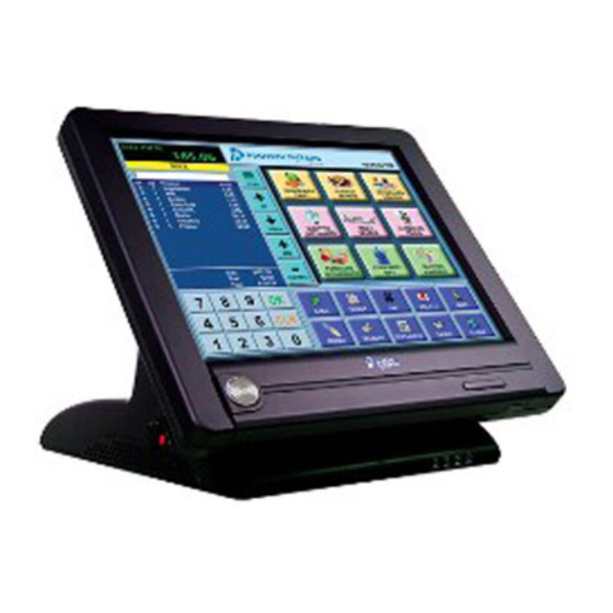
Page 9: Pos Illustration
Chapter 1 Introduction 1-2. POS SYSTEM ILLUSTRATION ′ Page: 1-3 PS-8851A USER S MANUAL... -
Page 10: System Specification
PC/AT Compatible, with mini DIN connecter on rear panel. MOUSE CONNECTOR : PS/2 Mouse, with mini DIN connecter on rear panel. IDE INTERFACE : one channel. 40-pin on-board connector for 3.5” Enhance DMA-33/66/100, standard type ′ Page: 1-4 PS-8851A USER S MANUAL... - Page 11 SOUND FUNCTION : VIA VT1612A, AC’ 97 Codec. Support Line-out (speaker)on Rear Panel. VGA FUNCTION : Built-in CLE266 supports LVDS (TFT panel) and RGB (CRT) signal BOARD DIMENSION : Prox-3251: 222mm x 192mm. ′ Page: 1-5 PS-8851A USER S MANUAL...
- Page 12 250 cd / m Signal Interface (bit) TTL (18-bit) LCD MTBF 30,000 Back Light MTBF (Hrs) 30,000 TOUCHSCREEN (OPTIONAL) RESISTIVE TYPE (5 wire) 1024 x 768 Resolution USB Interface Controller Power Consumption 10 million Durability (Lifetime) ′ Page: 1-6 PS-8851A USER S MANUAL...
- Page 13 DISK DRIVE HOUSING : One 3.5” HDD. HOUSING CONSTRUCTION: High quality plastic frame architecture DIMENSION : 315 x 356 x 277 mm (12.4” x 14” x 10.9”) NET WEIGHT : 8.7 kg (19.2lb) ′ Page: 1-7 PS-8851A USER S MANUAL...
-
Page 14: Safety Precautions
Do not install PS-8851A in the place that is extremely hot or cold. c. Avoid exposure to sunlight for a long period of time (for example in a closed car in summer time. - Page 15 Chapter 1 Introduction agent or with alcohol and then wipe thoroughly with a dry cloth. d. If dust has been accumulated on the outside, remove it by using a special made vacuum cleaner for computers. ′ Page: 1-9 PS-8851A USER S MANUAL...
-
Page 16: Chapter 2 System Configuration
CHAPTER SYSTEM CONFIGURATION Helpful information that describes the jumper & connector settings, and component locations. Section includes: Jumper & Connector Quick Reference Table Component Locations Configuration and Jumper settings Connector Pin Assignments Page 2-1... -
Page 17: Jumper & Connector Quick Reference Table
Onboard LAN Selection …………………………………... CMOS Function Selection ………………………………… JBAT1 LVDS Panel 3.3V/5V Voltage Selection ………………….. Memory Installation ..........…………. DIM1 PPCI Connector …………………………………………… PPCI1 Printer Port Connector …………………………………….. JLPT1 Reserved Pin ………………………………………………. JP10, JP14 Page: 2-2 ’ PS-8851A USER S MANUAL... -
Page 18: Component Locations
Chapter 2 Hardware Configuration 2-2. COMPONENT LOCATIONS PS-8851A Connector, Jumper and Component locations Page: 2-3 ’ PS-8851A USER S MANUAL... -
Page 19: How To Set The Jumpers
PIN1 & PIN2 to create one setting and shorting. You can either connect PIN2 & PIN3 to create another setting. The same jumper diagrams are applied all through this manual. The figure below shows what the manual diagrams look and what they represent. Page: 2-4 ’ PS-8851A USER S MANUAL... - Page 20 Chapter 2 Hardware Configuration JUMPER DIAGRAMS JUMPER SETTINGS Page: 2-5 ’ PS-8851A USER S MANUAL...
-
Page 21: Com Port Connector
ASSIGNMENT COM1_DCD COM1_RXD COM1_TXD COM1_DTR COM1_DSR COM1_RTS COM1_CTS COM1_RI/+5V/+12V selectable COM2 : COM2 Connector. The COM2 Connector assignments are as follows : ASSIGNMENT COM2_DCD COM2_RXD COM2_TXD COM2_DTR COM2_DSR COM2_RTS COM2_CTS COM2_ selectable RI/+5V/+12V Page: 2-6 ’ PS-8851A USER S MANUAL... - Page 22 ASSIGNMENT COM3_DCD COM3_RXD COM3_TXD COM3_DTR COM3_DSR COM3_RTS COM3_CTS COM3_ RI/+5V/+12V selectable COM4 : COM4 Connector. The pin assignments are as follows : ASSIGNMENT COM4_DCD COM4_RXD COM4_TXD COM4_DTR COM4_DSR COM4_RTS COM4_CTS COM4_ RI/+5V/+12V selectable Page: 2-7 ’ PS-8851A USER S MANUAL...
- Page 23 ASSIGNMENT COM4_ RI/+5V/+12V selectable COM4_ RI/+5V/+12V selectable COM4_DSR COM4_DTR COM4_RXD COM4_TXD All COM ports are selectable for RI, +5V or +12V. For more information, please refer to our “COM RI and Voltage Selection”. Page: 2-8 ’ PS-8851A USER S MANUAL...
-
Page 24: Com1Ri & Voltage Selection
Chapter 2 Hardware Configuration 2-5. COM1 RI & VOLTAGE SELECTION JP13 : COM1 RI & Voltage Selection. The selections are as follows: SELECTION JUMPER JUMPER SETTINGS ILLUSTRATION ***Manufacturing Default – RI. Page: 2-9 ’ PS-8851A USER S MANUAL... -
Page 25: Com2Ri & Voltage Selection
Chapter 2 Hardware Configuration 2-6. COM2 RI & VOLTAGE SELECTION JP6 : COM2 RI & Voltage Selection. The selections are as follows : SELECTION JUMPER JUMPER SETTINGS ILLUSTRATION ***Manufacturing Default – RI. Page: 2-10 ’ PS-8851A USER S MANUAL... -
Page 26: Com3Ri & Voltage Selection
Chapter 2 Hardware Configuration 2-7. COM3 RI & VOLTAGE SELECTION JP9 : COM3 RI & Voltage Selection. The selections are as follows : SELECTION JUMPER JUMPER SETTINGS ILLUSTRATION ***Manufacturing Default – RI. Page: 2-11 ’ PS-8851A USER S MANUAL... -
Page 27: Com4 Ri & Voltage Selection
Chapter 2 Hardware Configuration 2-8. COM4 and JCOM4 RI & VOLTAGE SELECTION JP4 : COM4 and JCOM4 RI & Voltage Selection. The selections are as follows : SELECTION JUMPER JUMPER SETTINGS ILLUSTRATION ***Manufacturing Default – RI. Page: 2-12 ’ PS-8851A USER S MANUAL... -
Page 28: Keyboard And Ps/2 Mouse Connector
SELECTION JP15 : PC/AT Keyboard and PS/2 Mouse 5V/5VSB Voltage Selection. The pin assignments are as follows : POWER JUMPER SETTING JUMPER TYPE (pin closed) ILLUSTRATION 5VSB ***Manufacturing Default is set as 5VSB. Page: 2-13 ’ PS-8851A USER S MANUAL... -
Page 29: Vga Connector
Chapter 2 Hardware Configuration 2-11. VGA CONNECTOR VGA1 : VGA Connector. The pin assignments are as follows : ASSIGNMENT GREEN BLUE VGA IIC DATA HSYNC VSYNC VGA IIC CLK Page: 2-14 ’ PS-8851A USER S MANUAL... -
Page 30: Audio Connector
ISOLATED GND LAN LED Indicator : Left side LED : Yellow Color Blinking LAN Message Active No LAN Message Active Right side LED : Green Color On LAN switch/hub connected No LAN switch/hub connected Page: 2-15 ’ PS-8851A USER S MANUAL... -
Page 31: Universal Serial Bus Connector
The pin assignment is as follows : ASSIGNMENT USBV2 USBC2- USBC2+ +12V JUSB2 : Universal Serial Bus Connector. The pin assignment is as follows : ASSIGNMENT ASSIGNMENT USBV3 USBV4 USBC3- USBC4- USBC3+ USBC4+ Page: 2-16 ’ PS-8851A USER S MANUAL... -
Page 32: Dc Jack
JPANEL1(1,3,5,7) : External Speaker Connector. The pin assignment is as follows : ASSIGNMENT SPKOUT SPK VCC 2-17. EXTERNAL SMI CONNECTOR JPANEL1(2,4) : External SMI# Connector. The pin assignment is as follows : ASSIGNMENT EXTSMIJ Page: 2-17 ’ PS-8851A USER S MANUAL... -
Page 33: Reset Button
Chapter 2 Hardware Configuration 2-18. RESET BUTTON JPANEL1(6,8) : Reset Button. The pin assignment is as follows : ASSIGNMENT RST_SW 2-19. POWER BUTTON PWBN1 : Power Button. The pin assignments are as follows: ASSIGNMENT PW_BN Page: 2-18 ’ PS-8851A USER S MANUAL... -
Page 34: Lvds Connector
LVDS1 : LVDS Connector. The pin assignments are as follows : ASSIGNMENT ASSIGNMENT LVDS_VCC CLKBM CLKBP YBM2 YBP2 YBM1 YBP1 YBP3 YBM3 YBP0 YBM0 CLKAP CLKAM YAP2 YAM2 YAP1 YAM1 YAP0 YAM0 YAP3 YAM3 LVDS_VCC LVDS_VCC Page: 2-19 ’ PS-8851A USER S MANUAL... -
Page 35: Lvds Panel Power Connector
IDERSTJ PDD7 PDD8 PDD6 PDD9 PDD5 PDD10 PDD4 PDD11 PDD3 PDD12 PDD2 PDD13 PDD1 PDD14 PDD0 PDD15 PDDREQ PDIOWJ PDIORJ PHDRDY PULL LOW PDDACKJ IDE_IRQ14 PDA1 GPIO PDA0 PDA2 PDCS1J PDCS3J IDE LED1J Page: 2-20 ’ PS-8851A USER S MANUAL... -
Page 36: Hdd Power Connector
The pin assignments are as follows : ASSIGNMENT +12V 2-24. CARD READER CONNECTOR JP8 : Card Reader Connector. The pin assignment is as follows : ASSIGNMENT +5V/5VSB selectable KB CLK KB CLK1 KB DATA KB DATA1 LINE_OUT_R LINE_OUT_L Page: 2-21 ’ PS-8851A USER S MANUAL... -
Page 37: System Fan Connector
2-26. Front Side LED CONNECTOR J2: Front Side LED Connector. The pin assignments are as follows : ASSIGNMENT PW_BN PULL HIGH to +3.3V HD_LED PULL HIGH to +3.3V ACTJ PULL HIGH to +3.3V SP100J Page: 2-22 ’ PS-8851A USER S MANUAL... -
Page 38: Onboard Lan Selection
To clear CMOS data, user must power-off the computer and set the jumper to “Clear CMOS” as the illustrated above. After five to six seconds, set the jumper back to “Normal” and power-on the computer. Page: 2-23 ’ PS-8851A USER S MANUAL... -
Page 39: Lvds Panel 3.3V/5V Voltage Selection
*** Manufacturing Default is +3.3V. 2-30. MEMORY INSTALLATION The system is enhanced with 1 DDR SDRAM bank, and the maximum capacity is 1GB. DRAM BANK CONFIGURATION DIM 1 TOTAL MEMORY 64MB 128M 128MB 256M 256MB 512M 512MB Page: 2-24 ’ PS-8851A USER S MANUAL... - Page 40 AD18 AD19 AD20 AD21 AD22 AD23 AD24 AD25 AD26 AD27 AD28 AD29 AD30 AD31 PLEDR PCICLK3 IRDYJ AD19 TRDYJ CBEJ0 CBEJ1 CBEJ2 CEBJ3 GNTJ3 REQJ3 SERRJ PERRJ INTRAJ PCIRSTXJ STOPJ PLOCKJ DEVSELJ FRAMEJ Page: 2-25 ’ PS-8851A USER S MANUAL...
- Page 41 Chapter 2 Hardware Configuration 2-32. PRINTER PORT CONNECTOR JLPT1 : Printer Port Connector. The pin assignments are as follows: ASSIGNMENT ASSIGNMENT STBJ AFDJ ERRJ INITJ SLINJ ACKJ BUSY SLCT Page: 2-26 ’ PS-8851A USER S MANUAL...
- Page 42 CHAPTER SOFTWARE UTILITIES This chapter comprises the detailed information of VGA driver, LAN driver, sound driver, VIA 4IN1 service pack driver, Touchscreen driver and Flash BIOS update. It also describes how to install the watchdog timer configuration. Section includes: VGA Driver Utility Flash BIOS Update LAN Driver Utility Sound Driver Utility...
- Page 43 Chapter 3 Software Configuration 3-1. INTRODUCTION PS-8851A driver utilities are contained in a CD ROM or Floppy Disk. For CD ROM disc user, you will only need some of the files contained in the CD ROM disc, please kindly refer to the following chart:...
- Page 44 Chapter 3 Software Configuration 3-2. VGA DRIVER UTILITY The VGA interface embedded with our PS-8851A can support a wide range of display mode, such as SVGA, STN, TFT ..etc. You can display CRT, LVDS and PanelLink simultaneously with the same mode.
- Page 45 Chapter 3 Software Configuration 3-3. FLASH BIOS UPDATE 3-3-1. System BIOS Update: Users of PS-8851A can use the program “Awdflash.exe” contained in the Utility Disk for system BIOS and VGA BIOS update. 3-3-2. To update VGA BIOS for LCD Flat Panel Display: You must update VGA BIOS in order to display with some specific LCD flat panel.
- Page 46 Flash Type - MXIC 29F002(N)T/5V File Name to Program: S75xxxxx.bin Checksum: XXXXX Reset System or Power off to accomplish update process! F1: Reset F10: Exit Please reset or power off the system to complete the BIOS update. ′ Page:3-5 PS-8851A USER S MANUAL...
- Page 47 Chapter 3 Software Configuration 3-4. LAN DRIVER UTILITY 3-4-1. Introduction PS-8851A Embedded Board is enhanced with LAN function that can support various network adapters. Installation programs for LAN drivers are listed as follows: 3-4-2. Installation Procedures of LAN Driver 1. Install LAN Driver to Windows 2000/XP Turn on the system, and Windows 2000/XP OS will detect the hardware automatically.
- Page 48 Last step to select OK and close NETWORK SETUP. Select SKIP if only one adapter is installed on this computer. For more information of installation procedure, please refer to TXT directory found on LAN DRIVER UTILITY. ′ Page:3-7 PS-8851A USER S MANUAL...
- Page 49 Windows 9x/98SE/ME, Windows NT, Linux, and Windows 2000/XP. Below, you will find the content of the Sound driver : 3-5-2. Installation Procedure To install, kindly refer to the readme.txt file on the Driver Disc (:\Sound\Realtek\Readme.txt). ′ Page:3-8 PS-8851A USER S MANUAL...
- Page 50 The VIA 4 In 1 driver includes four system drivers to improve the performance and maintain the stability of systems using VIA chipsets. These four drivers are: VIA Registry (INF) Driver, VIA AGP VxD driver, VIA ATAPI Vendor Support Driver and VIA PCI IRQ Miniport Driver ′ Page:3-9 PS-8851A USER S MANUAL...
- Page 51 Click Setup.exe file for USB driver installation. Follow the instructions on the screen to complete the installation. Once installation is completed, shut down the system and restart in order for the changes to take effect. ′ Page:3-10 PS-8851A USER S MANUAL...
- Page 52 CHAPTER AWARD BIOS SETUP This chapter shows how to set up the Award BIOS. Section includes: Introduction Entering Setup The Standard CMOS Features The Advanced BIOS Features The Advanced Chipset Features Integrated Peripherals Power Management Setup PNP/PCI Configuration PC Health Status Frequency/Voltage Control Load Fail-Safe Defaults Load Optimized Defaults...
- Page 53 4-1. INTRODUCTION This chapter will show you the function of the BIOS in managing the features of your system. The PS-8851A motherboard is equipped with the BIOS for system chipset from Award Software Inc. This page briefly explains the function of the BIOS in managing the special features of your system.
- Page 54 You may use the cursor the up/down keys to highlight the individual menu items. As you highlight each item, a brief description of the highlighted selection will appear at the bottom of the screen. ′ Page: 4-3 PS-8851A USER S MANUAL...
- Page 55 < Hour >, < Minute >, and < Second >. Use 24 hour clock format, i.e., for PM numbers, add 12 to the hour. For example: 4: 30 P.M. You should enter the time as 16:30:00. ′ Page: 4-4 PS-8851A USER S MANUAL...
- Page 56 Auto: The BIOS automatically determines the optimal mode. Normal: Maximum number of cylinders, heads, sectors supported are 1024, 16 and 63. Large: For drives that do not support LBA and have more than 1024 cylinders. ′ Page: 4-5 PS-8851A USER S MANUAL...
- Page 57 BASE MEMORY: Display the amount of conventional memory detected during boot up. EXTENDED MEMORY: Displays the amount of extended memory detected during boot up. TOTAL MEMORY: Displays the total memory available in the system. ′ Page: 4-6 PS-8851A USER S MANUAL...
- Page 58 1024 65535 1023 1024 65535 1023 1024 65535 1023 1024 65535 1023 1024 65535 1023 65535 1023 65535 1024 65535 1023 1024 65535 1023 65535 65535 65335 AUTO Award Hard Disk Type Table ′ Page: 4-7 PS-8851A USER S MANUAL...
- Page 59 The “BIOS FEATURES SETUP” allows you to configure your system for basic operation. User can select the system’s default speed, boot-up sequence, keyboard operation, shadowing and security. A brief introduction of each setting is given below. ′ Page: 4-8 PS-8851A USER S MANUAL...
- Page 60 For example, if you press and hold down the "A" key, the letter "a" will repeatedly appear on your screen until you release the key. When enabled, the typematic rate and typematic delay can be selected. ′ Page: 4-9 PS-8851A USER S MANUAL...
- Page 61 Select the operating system that is running with greater than 64MB of RAM on the system. VIDEO BIOS SHADOW: Determines whether video BIOS will be coped to RAM. However, it is optional depending on chipset design. Video Shadow will increase the video speed. ′ Page: 4-10 PS-8851A USER S MANUAL...
- Page 62 The default settings have been chosen because they provide the best opera- ting conditions for the system. The only time you might consider making any changes would be if you discovered that data was being lost while using your system. ′ Page: 4-11 PS-8851A USER S MANUAL...
- Page 63 The value in this field depends on performance parameters of the installed memory chips (DRAM). Do not change the value from the factory setting unless you install new memory that has a different performance rating than the original DRAMs. ′ Page: 4-12 PS-8851A USER S MANUAL...
- Page 64 This item allows you to adjust the AGP driving force. The Choice: Min=0000~ Max=00FF 4. AGP Master 1 WS Write When Enabled, writes to the AGP(Accelerated Graphics Port) are executed with one wait states.The choice: Enabled, Disabled ′ Page: 4-13 PS-8851A USER S MANUAL...
- Page 65 Select Enabled to support compliance with PCI specification version 2.1. MEMORY HOLE: In order to improve performance, certain space in memory can be reserved for ISA cards. This memory must be mapped into the memory space below 16MB. ′ Page: 4-14 PS-8851A USER S MANUAL...
- Page 66 VIDEO RAM CACHEABLE: Select Enabled allows caching of the video RAM , resulting in better system performance. However, if any program writes to this memory area, a system error may result. ′ Page: 4-15 PS-8851A USER S MANUAL...
- Page 67 Note: this cause just happen under Win9x, the phenomenon is a limitation. VIA ON-CHIP IDE DEVICE: You could expand the whole menu by pressing <ENTER>, and you will see a screen like the one listed below: ′ Page: 4-16 PS-8851A USER S MANUAL...
- Page 68 (0-4) for each of the four IDE devices that the onboard IDE interface supports. Modes 0 through 4 provide successively increased performance. In Auto mode, the system automatically determines the best mode for each device. ′ Page: 4-17 PS-8851A USER S MANUAL...
- Page 69 Select enabled if the system contains a Universal Serial Bus (USB) controller and you have a USB peripherals. USB Keyboard Support Select enabled if the system contains a Universal Serial Bus (USB) controller and you have a USB Keyboard. ′ Page: 4-18 PS-8851A USER S MANUAL...
- Page 70 2. Onboard Serial Port 1/2/3/4 Select an address and corresponding interrupt for the first and second serial ports. 3. UART Mode Select This item allows you to select UART mode. 4. UR2 Duplex Mode ′ Page: 4-19 PS-8851A USER S MANUAL...
- Page 71 8. ECP Mode Use DMA Select a DMA channel for the parallel port for use during ECP mode. INIT DISPLAY FIRST: This item allows you to decide to active whether PCI Slot or on-chip VGA first. ′ Page: 4-20 PS-8851A USER S MANUAL...
- Page 72 There are four available options: Disable, Min. Power Saving, Max. Power Saving, and User Define. SUSPEND MODE: When enabled and after the set time of system inactivity, all devices except the CPU will be shut off. ′ Page: 4-21 PS-8851A USER S MANUAL...
- Page 73 In effect, the system remains alert for anything that occurs to a device, which is configured as ON, even when the system is in a power down mode. VGA: When Enabled, you can set the VGA awakens the system. ′ Page: 4-22 PS-8851A USER S MANUAL...
- Page 74 When Enabled, you can set the date and the time at which the RTC alarm awakens the system from Suspend mode. PRIMARY INTR: When set to Off, IRQ Activity Monitoring is set to BIOS default. When set to On, user may select the desired setting. ′ Page: 4-23 PS-8851A USER S MANUAL...
- Page 75 Normally, you leave this field Disabled. Select Enabled to reset Extended System Configuration Data (ESCD) when you exit Setup if you have installed a new add-on and the system configuration has caused such a serious conflict that the operating system cannot boot. ′ Page: 4-24 PS-8851A USER S MANUAL...
- Page 76 DMA channel. PCI/VGA PALETTE SNOOP: Leave this field at disabled. ASSIGN IRQ FOR VGA: This item Enable/Disable to assign IRQ for VGA. ASSIGN IRQ FOR USB: This item Enable/Disable to assign IRQ for USB. ′ Page: 4-25 PS-8851A USER S MANUAL...
- Page 77 This item shows you the current system voltage. +3.3V/+5V/+12V/-12V: This item shows you the voltage status of +3.3V/+5V/+12V/-12V. SHUTDOWN TEMPERATURE: This item allows you to set the CPU shutdown Temperature. This function is only effective under Window 98 ACPI mode. ′ Page: 4-26 PS-8851A USER S MANUAL...
- Page 78 SCSI device. CPU RATIO: This item allows you to set up the CPU clock ratio, but this function depends on different CPU performance. It is only effective for those clock ratio haven’t been locked. ′ Page: 4-27 PS-8851A USER S MANUAL...
- Page 79 Load Optimized Defaults ( Y/N ) ? N To restore the optimal BIOS configuration, please click "Y" and press "Enter".BIOS will be restored after you restart the system. ′ Page: 4-28 PS-8851A USER S MANUAL...
- Page 80 PASSWORD DISABLED!!! Press any key to continue... Press the < Enter > key again and the password will be disabled. Once the password is disabled, you can enter Setup freely. ′ Page: 4-29 PS-8851A USER S MANUAL...
- Page 81 You may always call up the setup program at any time to adjust any of the individual items by pressing the <Del> key during boot up. ′ Page: 4-30 PS-8851A USER S MANUAL...
- Page 82 ►Integrated Peripherals ►Power Management word Quit Without Saving (Y/N)? N ►PnP/PCI Configura etup ►PC Health Status Saving Esc : Quit ↑↓→← : Select Item F10 : Save & Exit Setup Abandon all Datas ′ Page: 4-31 PS-8851A USER S MANUAL...
-
Page 83: Appendix A System Assembly
APPENDIX SYSTEM ASSEMBLY This appendix contain exploded diagram of the system. Section includes: Exploded Diagram for LCD Exploded Diagram for System Base Unit Exploded Diagram for 3.5” Hard Disk Drive and Bottom Cover Exploded Diagram for Bottom Cover and System Fan Exploded Diagram for Customer Display Installation Page: A-1... -
Page 84: Exploded Diagram For Lcd
Appendix A System Assembly EXPLODED DIAGRAM FOR LCD STEP 1: Rotate the LCD to horizontal. STEP 2: Loose two screws. STEP3: Push the LCD forward, and then lift up. (Front) ′ Page: A-2 PS-8851A USER S MANUAL... - Page 85 Appendix A System Assembly STEP 4: Make the LCD to stand up, and then remove all the screws and cables. (Back) ′ Page: A-3 PS-8851A USER S MANUAL...
-
Page 86: Exploded Diagram For System Base Unit
Appendix A System Assembly EXPLODED DIAGRAM FOR SYSTEM BASE UNIT Diagram 1: ′ Page: A-4 PS-8851A USER S MANUAL... - Page 87 Appendix A System Assembly Diagram 2: ′ Page: A-5 PS-8851A USER S MANUAL...
-
Page 88: Exploded Diagram For 3.5" Hard Disk Drive And Bottom Cover
Appendix A System Assembly EXPLODED DIAGRAM FOR 3.5” HARD DISK DRIVE AND BUTTOM COVER ′ Page: A-6 PS-8851A USER S MANUAL... -
Page 89: Exploded Diagram For Bottom Cover And System Fan
Appendix A System Assembly EXPLODED DIAGRAM FOR BOTTOM COVER AND SYSTEM ′ Page: A-7 PS-8851A USER S MANUAL... -
Page 90: Exploded Diagram For Customer Display Installation
Appendix A System Assembly EXPLODED DIAGRAM FOR CUSTOMER DISPLAY INSTALLATION STEP 1: From the bottom, remove 2 screws (like A). (Bottom) ′ Page: A-8 PS-8851A USER S MANUAL... - Page 91 Appendix A System Assembly STEP 2: Remove Elliptic cover (location 2). (Back) ′ Page: A-9 PS-8851A USER S MANUAL...
- Page 92 Appendix A System Assembly STEP 3: Put cable into olive hole. STEP 4: Plug in the customer display. STEP 5: Tight the screws. (Back) ′ Page: A-10 PS-8851A USER S MANUAL...
- Page 93 Warning: When the PS8851A shipment bundled with LCD customer display “PS8710”, the COM4 default will be set to “12V”. (Please note the 12V voltage may damage the COM port device without voltage required.) ′ Page: A-11 PS-8851A USER S MANUAL...
- Page 94 Appendix A System Assembly EXPLODED DIAGRAM OF CUSTOMER DISPLAY ′ Page: A-12 PS-8851A USER S MANUAL...
- Page 95 APPENDIX TECHNICAL SUMMARY This section introduces you the maps concisely. Section includes: Block Diagram Interrupt Map RTC (Standard) RAM Bank Timer & DMA Channels Map I / O & Memory Map Page: B-1...
-
Page 96: Appendix B Technical Summary Block Diagram
Appendix B Technical Summary BLOCK DIAGRAM ′ Page: B-2 PS-8851A USER S MANUAL... -
Page 97: Interrupt Map
System TIMER interrupt from TIMER-0 Keyboard Cascade for IRQ 8-15 Serial port 2 Serial port 1 Parallel port 2 Floppy disk Parallel port 1 RTC Alarm clock IRQ2 Redir COM3 COM4 PS/2 Mouse Coprocessor IDE1 IDE2 ′ Page: B-3 PS-8851A USER S MANUAL... -
Page 98: Rtc & Cmos Ram Map
Extension memory low byte Extension memory high byte Reserved for extension memory low byte Reserved for extension memory high byte Date Century byte Information Flag 34-3F Reserve 40-7f Reserved for Chipset Setting Data ′ Page: B-4 PS-8851A USER S MANUAL... -
Page 99: Timer & Dma Channels Map
Timer Channel Map : Timer Channel Assignment System timer interrupt DRAM Refresh request Speaker tone generator DMA Channel Map : DMA Channel Assignment Available Available Floppy Available Cascade for DMA controller 1 Available Available Available ′ Page: B-5 PS-8851A USER S MANUAL... -
Page 100: I/O & Memory Map
Parallel port-2 2B0-2DF Graphics adapter controller 2F8-2FF Serial port-2 360-36F Net work ports 378-37F Parallel port-1 3B0-3BF Monochrome & Printer adapter 3C0-3CF EGA adapter 3D0-3DF CGA adapter 3F0-3F7 Floppy disk controller 3F8-3FF Serial port-1 ′ Page: B-6 PS-8851A USER S MANUAL...
Need help?
Do you have a question about the PS-8851A and is the answer not in the manual?
Questions and answers