Table of Contents
Advertisement
Quick Links
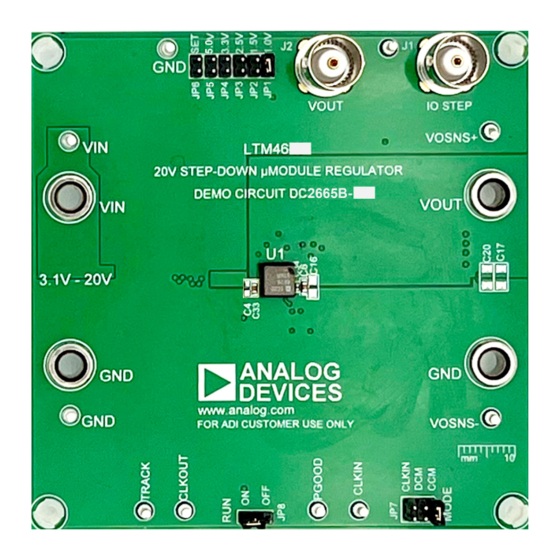
DESCRIPTION
Demonstration circuit 2665B-C features the
µModule
regulator, a high performance, high efficiency
®
step-down regulator. The LTM4657 is a complete DC/DC
point-of-load regulator in a thermally enhanced 6.25mm
× 6.25mm × 3.87mm BGA package. The LTM4657 has an
operating input voltage range of 3.1V to 20V and provides
an output current up to 8A. The output voltage is program-
mable from 0.5V to 5.5V and can be remotely sensed.
The stacked inductor design improves thermal dissipa-
tion and significantly reduces the package area. Output
BOARD PHOTO
LTM
4657
®
Part marking is either ink mark or laser mark
DEMO MANUAL DC2665B-C
20V
µModule Regulator
voltage tracking is available through the TRACK/ SS pin
for supply rail sequencing. External clock synchronization
is available through the SYNC/MODE pin. For high effi-
ciency at low load currents, select discontinuous current
mode (DCM) operation using the MODE jumper (JP7) in
less noise sensitive applications. Refer to the LTM4657
data sheet in conjunction with this demo manual for
working on or modifying DC2665B-C.
Design files for this circuit board are
All registered trademarks and trademarks are the property of their respective owners.
LTM4657
8A Step-Down
IN,
available.
Rev. 0
1
Advertisement
Table of Contents

Subscribe to Our Youtube Channel
Related Manuals for Analog Devices DC2665B-C


Summary of Contents for Analog Devices DC2665B-C
- Page 1 8A. The output voltage is program- data sheet in conjunction with this demo manual for mable from 0.5V to 5.5V and can be remotely sensed. working on or modifying DC2665B-C. The stacked inductor design improves thermal dissipa- Design files for this circuit board are available.
-
Page 2: Performance Summary
DEMO MANUAL DC2665B-C PERFORMANCE SUMMARY Specifications are at T = 25°C PARAMETER CONDITIONS UNITS Input Voltage Range Output Voltage, V Jumper Selection on JP1 0.98 1.02 Jumper Selection on JP2 1.47 1.53 Jumper Selection on JP3 2.45 2.55 Jumper Selection on JP4 3.23... - Page 3 DEMO MANUAL DC2665B-C QUICK START PROCEDURE dc2665bc F01 Figure 1. Test Setup of DC2665B-C NOTES: 1. To achieve the minimum output ripple voltage, optimize the operation frequency at different input and output volt- ages. Suggested operation frequencies at different voltages are shown in Table 1. Adjust the operation frequency by changing the value of R (R5).
- Page 4 DEMO MANUAL DC2665B-C QUICK START PROCEDURE , 500kHz , 500kHz 1.5V , 650kHz 1.5V , 650kHz 2.5V , 800kHz , 500kHz 2.5V , 800kHz 3.3V , 1MHz 1.5V , 650kHz 3.3V , 1MHz , 1.25MHz 2.5V , 800kHz LOAD CURRENT (A)
- Page 5 DEMO MANUAL DC2665B-C QUICK START PROCEDURE QUICK START PROCEDURE 20mV/DIV LOAD 1A/DIV dc2665bc F04a 40 s/DIV = 28mV OUT(PK-PK) (a) 1V 20mV/DIV LOAD 1A/DIV dc2665bc F04b 40 s/DIV = 32.8mV OUT(PK-PK) (b) 5V Figure 4. Load Transient (4A to 6A) Response Waveform at 12V...
-
Page 6: Parts List
DEMO MANUAL DC2665B-C QUICK START PROCEDURE 10mV/DIV 10mV/DIV dc2665bc F05b dc2665bc F05a 1 s/DIV 1 s/DIV = 6.8mV = 20mV OUT(PK-PK) OUT(PK-PK) (a) 1V , 500kHz, Full Bandwidth at 500MHz (b) 1V , 500kHz, 20MHz Bandwidth 10mV/DIV 10mV/DIV dc2665bc F05c... - Page 7 DEMO MANUAL DC2665B-C PARTS LIST ITEM REFERENCE PART DESCRIPTION MANUFACTURER/PART NUMBER CAP ., 1μF, X7R, 6.3V, 10%, 0402 MURATA, GRM155R70J105KA12D RES., 10k, 1%, 1/10W, 0603 VISHAY, CRCW060310K0FKEAC RES., 60.4k, 1%, 1/10W, 0603 VISHAY, CRCW060360K4FKEA RES., 30.1k, 1%, 1/10W, 0603 VISHAY, CRCW060330K1FKEA RES., 10.7k, 1%, 1/10W, 0603...
-
Page 8: Schematic Diagram
DEMO MANUAL DC2665B-C SCHEMATIC DIAGRAM Rev. 0... -
Page 9: Revision History
Devices for its use, nor for any infringements of patents or other rights of third parties that may result from its use. Specifications subject to change without notice. No license is granted by implication or otherwise under any patent or patent rights of Analog Devices. - Page 10 Board until you have read and agreed to the Agreement. Your use of the Evaluation Board shall signify your acceptance of the Agreement. This Agreement is made by and between you (“Customer”) and Analog Devices, Inc. (“ADI”), with its principal place of business at One Technology Way, Norwood, MA 02062, USA. Subject to the terms and conditions of the Agreement, ADI hereby grants to Customer a free, limited, personal, temporary, non-exclusive, non-sublicensable, non-transferable license to use the Evaluation Board FOR EVALUATION PURPOSES ONLY.
Need help?
Do you have a question about the DC2665B-C and is the answer not in the manual?
Questions and answers