Advertisement
Quick Links
Description
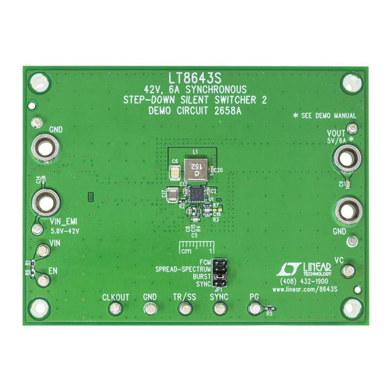
Demonstration circuit 2658A is a 42V, 6A synchronous
step-down second generation SILENT SWITCHER with
spread spectrum frequency modulation featuring the
LT
8643S. The demo board is designed for 5V output
®
from a 5.8V to 42V input. The wide input range allows a
variety of input sources, such as automotive batteries and
industrial supplies. The LT8643S is a compact, ultralow
emission, high efficiency, and high speed synchronous
monolithic step-down switching regulator. The integrated
bypass capacitors optimize all the fast current loops and
make it easier to minimize EMI/EMC emissions by reducing
layout sensitivity. Selectable spread spectrum mode can
further improve EMI/EMC performance. Fast minimum
on-time of 30ns enables high V
at high frequency.
The LT8643S switching frequency can be programmed
either via oscillator resistor or external clock over a
200kHz to 3MHz range. The default frequency of demo
circuit 2658A is 2MHz. The SYNC pin on the demo board
is grounded (JP1 at BURST position) by default for low
ripple burst mode operation. To synchronize to an external
clock, move JP1 to SYNC and apply the external clock to
the SYNC terminal. Spread spectrum mode and forced
continuous mode can be selected respectively by moving
JP1 shunt. Figure 1 shows the efficiency of the circuit at
12V input and 24V input in Burst Mode Operation (input
terminal to bypass the EMI filter). Figure 2 shows
from V
IN
performance summary
SYMBOL
PARAMETER
V
Input Supply Range with EMI Filter
IN_EMI
V
Output Voltage
OUT
I
Maximum Output Current
OUT
f
Switching Frequency
SW
EFF
Efficiency
Arrow.com.
Downloaded from
to low V
conversion
IN
OUT
Specifications are at T
CONDITIONS
Derating Is Necessary for Certain V
Thermal Conditions
V
= 12V , I
IN
OUT
DEMO MANUAL DC2658A
42V, 6A Synchronous
Step-Down Silent Switcher 2
the LT8643S temperature rising on DC2658A demo board
under different load conditions. The rated maximum load
current is 6A, while derating is necessary for certain input
voltage and thermal conditions.
The demo board has an EMI filter installed. The EMI perfor-
mance of the board (with EMI filter) is shown on Figure 3.
The red line in Radiated EMI Performance is CISPR25 Class
5 peak limit. The figure shows that the circuit passes the
test with a wide margin. To achieve EMI/EMC performance
as shown in Figure 3, the input EMI filter is required and
the input voltage should be applied at VIN_EMI terminal.
An inductor can be added in the EMI filter to further reduce
the conducted emission. The EMI filter can be bypassed
by applying the input voltage at V
The LT8643S data sheet gives a complete description
of the part, operation and application information. The
data sheet must be read in conjunction with this demo
manual for DC2658A. The LT8643S is assembled in a
4mm × 4mm LQFN package with exposed pads for low
thermal resistance. The layout recommendations for low
EMI operation and maximum thermal performance are
available in the data sheet section Low EMI PCB Layout
and Thermal Considerations and Peak Output Current.
Design files for this circuit board are available at
http://www.linear.com/demo/DC2658A
L, LT, LTC, LTM, Linear Technology and the Linear logo are registered trademarks of Linear
Technology Corporation. All other trademarks are the property of their respective owners.
= 25°C
A
and
IN
= 3A
LT8643S
terminal.
IN
MIN
TYP
MAX
5.8
42
4.85
5
5.15
6
1.85
2
2.15
94.2
UNITS
V
V
A
MHz
%
dc2658af
1
Advertisement

Subscribe to Our Youtube Channel
Related Manuals for Analog Devices Linear Technology 2658A


Summary of Contents for Analog Devices Linear Technology 2658A
- Page 1 DEMO MANUAL DC2658A LT8643S 42V, 6A Synchronous Step-Down Silent Switcher 2 Description Demonstration circuit 2658A is a 42V, 6A synchronous the LT8643S temperature rising on DC2658A demo board step-down second generation SILENT SWITCHER with under different load conditions. The rated maximum load spread spectrum frequency modulation featuring the current is 6A, while derating is necessary for certain input 8643S.
- Page 2 DEMO MANUAL DC2658A EFFICIENCY = 12V = 24V POWER LOSS = 5V = 6A = 5V = 2MHz = 5A = 2MHz SYNC/MODE = GND = 4A 0.5 1 1.5 2 2.5 3 3.5 4 4.5 5 5.5 6 LOAD CURRENT (A) INPUT VOLTAGE (V) DC2658A F01 DC2658A F02...
- Page 3 DEMO MANUAL DC2658A Conducted EMI Performance –10 –20 SPREAD SPECTRUM MODE –30 FIXED FREQUENCY MODE –40 FREQUENCY (MHz) DC2658 F03a (WITH EMI FILTER INSTALLED) 14V INPUT TO 5V OUTPUT AT 4A, f = 2MHz Radiated EMI Performance (CISPR25 Radiated Emission Test with Class 5 Peak Limits) VERTICAL POLARIZATION PEAK DETECTOR CLASS 5 PEAK LIMIT...
-
Page 4: Quick Start Procedure
DEMO MANUAL DC2658A Quick start proceDure Demonstration circuit 2658A is easy to set up to evalu- 5. Check for the proper output voltage (V = 5V). ate the performance of the LT8643S. Refer to Figure 4 NOTE: If there is no output, temporarily disconnect the for proper measurement equipment setup and follow the load to make sure that the load is not set too high or is procedure below:... - Page 5 DEMO MANUAL DC2658A Quick start proceDure Figure 5. Measuring Output Ripple at Output Capacitor C9 5mV/DIV AC-COUPLED DC2658A F06 500ns/DIV Figure 6. LT8643S Demo Circuit DC2658A Output Voltage Ripple (12V Input, I = 6A, Full BW) dc2658af Arrow.com. Arrow.com. Arrow.com. Arrow.com.
-
Page 6: Parts List
DEMO MANUAL DC2658A parts List ITEM REFERENCE PART DESCRIPTION MANUFACTURER/PART NUMBER Required Circuit Components C2, C12 CAP ., X5R, 1μF, 50V, 10%, 0603 MURATA, GRM188R61H105KAALD CAP ., C0G, 330pF, 50V, 5%, 0603 MURATA, GRM1885C1H331JA01D CAP ., X5R, 100μF, 10V, 20% 1210 MURATA, GRM32ER61A107ME20L CAP ., X7R, 0.1μF, 16V, 10%, 0603 MURATA, GRM188R71C104KA01D... -
Page 7: Schematic Diagram
DEMO MANUAL DC2658A schematic Diagram dc2658af Information furnished by Linear Technology Corporation is believed to be accurate and reliable. However, no responsibility is assumed for its use. Linear Technology Corporation makes no representa- tion that the interconnection of its circuits as described herein will not infringe on existing patent rights. Arrow.com. - Page 8 DEMO MANUAL DC2658A DEMONSTRATION BOARD IMPORTANT NOTICE Linear Technology Corporation (LTC) provides the enclosed product(s) under the following AS IS conditions: This demonstration board (DEMO BOARD) kit being sold or provided by Linear Technology is intended for use for ENGINEERING DEVELOPMENT OR EVALUATION PURPOSES ONLY and is not provided by LTC for commercial use.
Need help?
Do you have a question about the Linear Technology 2658A and is the answer not in the manual?
Questions and answers