Table of Contents
Advertisement
Quick Links
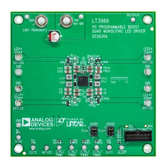
DESCRIPTION
Demonstration circuit 2630A is an I
quad channel monolithic boost LED driver featuring the
LT
3966. It drives four separate strings of LEDs (up
®
to 50V) at 125mA when V
DC2630A runs at 2MHz switching frequency. Its four
channels are capable of powering LED strings which can
have different currents, voltages, or dimming ratios. Each
channel can be independently controlled via I
nications or analog inputs. DC2630A can be configured to
run in either mode by modifying the ADDR pin settings.
It is protected against output overcurrent, overvoltage
events, and reports open and short LED fault events by
2
latching an alert pin. In I
disabled. A DC2026C Linduino
is used to interface with the board by directly connecting
it with a QuikEval™ ribbon cable and provided command
line interface code.
The LT3966 has an input voltage range from 3V to 60V.
Each boost channel has an integrated 60V 1.6A low-side
power switch. It has adjustable switching frequency
between 300kHz and 2MHz and can be synchronized to
an external clock source. Additionally, LT3966 can be pro-
grammed to output its own master clock to sync other
devices. The high side PWMTG MOSFET drivers assist
with PWM dimming and fault protection. The LT3966
channels can be configured to operate as a ground-ref-
erenced step-up (boost) LED driver, or as a floating output
LED driver to perform step-down (buck mode) or step-up/
step-down (buck-boost mode) operation.
2
C programmable
is between 9V and 18V.
IN
2
C commu-
C mode, faults can be enabled or
One demonstration circuit
®
DEMO MANUAL DC2630A
2
I
C Programmable Quad
Monolithic Boost LED Driver
Each channel of the LT3966 can be independently dimmed
by applying a PWM signal or CTRL voltage to the corre-
sponding channel CTRL/PWM pin while operating in non-
2
2
I
C mode. In I
C mode, each channel has a maximum of
13 bits of PWM dimming resolution and 8 bits of analog
dimming resolution.
Small ceramic input and output capacitors are used to
save space and cost. The open LED overvoltage protection
uses the IC's constant-voltage regulation loop to regu-
late the output to approximately 57V if the LED string
is opened.
Undervoltage lockout can be adjusted on the circuit with a
few simple resistor choices. The output voltage (overvolt-
age protection) can be adjusted by changing the feedback
resistors for different string voltages. Other components
may need to be changed to accommodate the change in
output voltages as well.
The LT3966 data sheet gives a complete description of
the device, operation and applications information. The
data sheet must be read in conjunction with this demo
manual for DC2630A. The LT3966EUJ is assembled in a
40-lead plastic 6mm × 6mm QFN package with a thermally
enhanced ground.
Design files for this circuit board are
All registered trademarks and trademarks are the property of their respective owners.
LT3966
available.
Rev. 0
1
Advertisement
Table of Contents

Subscribe to Our Youtube Channel
Related Manuals for Analog Devices DC2630A


Summary of Contents for Analog Devices DC2630A
- Page 1 I C commu- save space and cost. The open LED overvoltage protection nications or analog inputs. DC2630A can be configured to uses the IC’s constant-voltage regulation loop to regu- run in either mode by modifying the ADDR pin settings.
- Page 2 0V and 1.5V. See data sheet HOW TO OPERATE DC2630A IN NON-I C MODE for details. The DC2630A is easy to set up to evaluate the perfor- 7. To change brightness with external PWM dimming mance of the LT3966 in non-I C mode. Refer to Figure 1...
- Page 3 C serial communications, set JP1 (ADDR1) the DC2630A web page. to 1 and JP2 (ADDR2) to 1. This is the chosen I address for the DC2630A command line interface. 5. Upload the code to the connected Linduino demo circuit. 8. Open up the serial monitor inside Arduino IDE.
- Page 4 DEMO MANUAL DC2630A TEST RESULTS dc2630a F02 Figure 2. DC2630A Input Voltage vs Efficiency – 4× Channels Powering 16 White LEDs Per Channel at 125mA 244Hz PWM FREQUENCY 50mA/DIV 500:1 1250:1 dc2630a F03 1µs/DIV Figure 3. DC2630A PWM Dimming Using I C Settings for 1250:1 and 500:1 Dimming Ratios...
- Page 5 DEMO MANUAL DC2630A TEST RESULTS CTRL/PWM 500mV/DIV 50mA/DIV dc2630a F04a 20µs/DIV (a) 50% to 100% CTRL/PWM 500mV/DIV 50mA/DIV dc2630a F04b 20µs/DIV (b) 100% to 50% Figure 4. DC2630A Load Transient Response Rev. 0...
- Page 6 DEMO MANUAL DC2630A PARTS LIST ITEM QTY REFERENCE PART DESCRIPTION MANUFACTURER/PART NUMBER Required Circuit Components C1, C2, C7, C8, C11, C12, C15, C16 CAP ., X7R, 2.2µF, 50V, 10% 1206 AVX, 12065C225KAT2A C4, C5, C9, C10, C13, C14, C17, C18 CAP ., X7R, 2.2µF, 100V, 10% 1206 AVX, 12061C225KAT4A CAP ., X5R, 4.7µF, 16V, 10% 0603...
- Page 7 Devices for its use, nor for any infringements of patents or other rights of third parties that may result from its use. Specifications subject to change without notice. No license is granted by implication or otherwise under any patent or patent rights of Analog Devices.
- Page 8 Board until you have read and agreed to the Agreement. Your use of the Evaluation Board shall signify your acceptance of the Agreement. This Agreement is made by and between you (“Customer”) and Analog Devices, Inc. (“ADI”), with its principal place of business at One Technology Way, Norwood, MA 02062, USA. Subject to the terms and conditions of the Agreement, ADI hereby grants to Customer a free, limited, personal, temporary, non-exclusive, non-sublicensable, non-transferable license to use the Evaluation Board FOR EVALUATION PURPOSES ONLY.
Need help?
Do you have a question about the DC2630A and is the answer not in the manual?
Questions and answers