Advertisement
Buck Converter with Boost Channel as SEPIC
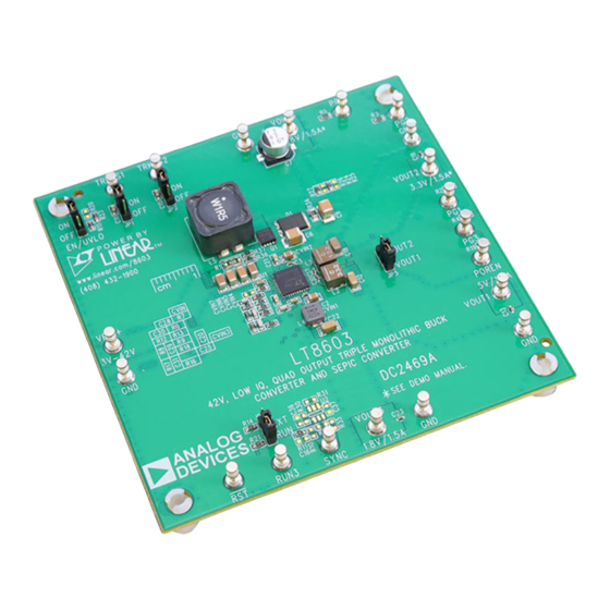
DESCRIPTION
Demonstration circuit 2469A features the
triple monolithic buck regulators and the boost channel as
SEPIC. The demo circuit is designed for 8V, 5V, 3.3V, and
1.8V outputs from a nominal 12V input. The 4th channel is
set as a SEPIC converter and its output is regulated at 8V
over a wide input range. The two high voltage buck regula-
tors are powered from VOUT4. VOUT1 is regulated at 5V
with 1.5A maximum output load current, and VOUT2 is
at 3.3V with 2.5A maximum output load current. The low
voltage buck is powered from VOUT2 (3.3V), and the out-
put VOUT3 is regulated at 1.8V with 1.8A maximum load
current. Thanks to the SEPIC converter, all four outputs
can ride through a cold crank in automotive applications
while providing regulated output voltages.
All regulators are synchronized to an internal oscillator
that can be programmed with one resistor at RT pin.
Programmable frequency allows optimization between
efficiency and external component size. To avoid the audio
band, the DC2469A sets the switching frequency at 2MHz
for the three buck regulators, and the SEPIC converter is
at 400kHz. At all frequencies, a 180° phase shift is main-
tained between 1 and 2 channels, reducing the input peak
current and voltage ripple.
PERFORMANCE SUMMARY
Table 1.
PARAMETER
Operation Input Voltage Range
Minimum Start-Up, VIN
MIN
Standby Current When Switching
Channel 4 Output Voltage, VOUT4
Channel 1 Output Voltage, VOUT1
Channel 2 Output Voltage, VOUT2
Channel 3 Output Voltage, VOUT3
Maximum Output Current, IOUT1
Maximum Output Current, IOUT2
42V, Low I
, Quad Output Triple Monolithic
Q
LT
8603
with
®
Specifications are at T
CONDITIONS
IOUT1,2,3,4 = 0mA, V
IOUT4 = 1A
IOUT1 = 1.5A
IOUT2 = 2.5A
IOUT3 = 1.8A
V
= 12V
IN
V
= 12V, IOUT3 = 0A
IN
DEMO MANUAL DC2469A
Many popular features such as soft-start, cycle-by-cycle
current limit, power good for each of the four channels
are packed in the 40-lead 6mm × 6mm QFN package to
simplify the complex design of quad-output power con-
verters. Each buck regulator can be independently dis-
abled using its own TRKSS or RUN pin. The SEPIC can be
disabled by pulling down both the FSEL4A and FSEL4B.
The EN/UVLO can be used to shut down the circuit to
reduce the input current to 1µA.
Table 1 summarizes the performance of the demo board at
room temperature. The demo circuit can be easily modi-
fied for various automotive, transportation and industry
applications. For applications that need 4th channel con-
figured as a boost converter, the DC2114A should be used.
The LT8603 data sheet gives a complete description of
the part, operation and application information. The data
sheet must be read in conjunction with this quick start
guide for DC2469A.
Design files for this circuit board are available at
http://www.linear.com/demo/DC2469A
All registered trademarks and trademarks are the property of their respective owners.
= 25°C
A
= 12V
IN
LT8603
MIN
TYP
MAX
3
12
42
4.5
40
7.68
8
8.32
4.86
5
5.14
3.17
3.3
3.43
1.73
1.8
1.87
1.5
2.5
UNITS
V
V
µA
V
V
V
V
A
A
dc2469af
1
Advertisement
Table of Contents

Subscribe to Our Youtube Channel
Related Manuals for Analog Devices LINEAR DC2469A


Summary of Contents for Analog Devices LINEAR DC2469A
- Page 1 DEMO MANUAL DC2469A LT8603 42V, Low I , Quad Output Triple Monolithic Buck Converter with Boost Channel as SEPIC DESCRIPTION Demonstration circuit 2469A features the 8603 with Many popular features such as soft-start, cycle-by-cycle ® triple monolithic buck regulators and the boost channel as current limit, power good for each of the four channels SEPIC.
-
Page 2: Performance Summary
DEMO MANUAL DC2469A PERFORMANCE SUMMARY Table 1. PARAMETER CONDITIONS UNITS Maximum Output Current, IOUT3 = 12V, IOUT2 = 0A Maximum Output Current, IOUT4 = 12V, IOUT1,2,3 = 0A Switching Frequency, Channel 1~3 = 12V, IOUT1,2,3 = 1A 1.85 2.15 Switching Frequency, Channel 4 = 6V, IOUT4 = 1A Efficiency, Channel 4 = 7V, IOUT4 = 2.5A... - Page 3 DEMO MANUAL DC2469A QUICK START PROCEDURE loads are not set too high, and the headers of EN/UVLO, 6. When measuring the input or output voltage ripples, TRKSS1, TRKSS2, RUN3 are set in right positions. care must be taken to avoid a long ground lead on the oscilloscope probe.
- Page 4 DEMO MANUAL DC2469A QUICK START PROCEDURE Figure 1. Proper Measurement Equipment Setup dc2469af...
- Page 5 DEMO MANUAL DC2469A QUICK START PROCEDURE OR V Figure 2. Proper Scope Probe Placement for Measuring Input or Output Ripple A) V = 6V B) V = 24V Figure 3. Thermal Image Top View, IOUT1 = 1A, IOUT2 = 1A, IOUT3 = 1A, T = 25°C, F = 2MHz dc2469af...
- Page 6 DEMO MANUAL DC2469A QUICK START PROCEDURE CH1, CH2 Efficiency Efficiency, V = 8V Burst Mode OPERATION PULSE-SKIPPING MODE = 2MHz = 8V = 400kHz = 7V 0 0.3 0.5 0.8 1 1.3 1.5 1.8 2 2.3 2.5 0 0.3 0.5 0.8 1 1.3 1.5 1.8 2 2.3 2.5 LOAD CURRENT (A) LOAD CURRENT (A) DC2469A F04a...
-
Page 7: Parts List
DEMO MANUAL DC2469A PARTS LIST ITEM REFERENCE PART DESCRIPTION MANUFACTURER/PART NUMBER Required Circuit Components CVIN Cap, X5R 1µF 50V 10% 0603 Murata, GRM188R61H105KAALD C26, C27 Cap, X7R 4.7µF 50V 10% 1206 Murata, GRM31CR71H475KA12L CVIN1, CVIN2 Cap, X7R 4.7µF 16V 10% 0805 Murata, GRM21BR71C475KA73L CVIN3 Cap, X5R 10µF 6.3V 20% 0603... - Page 8 DEMO MANUAL DC2469A PARTS LIST ITEM REFERENCE PART DESCRIPTION MANUFACTURER/PART NUMBER Res, Chip 2.49M 0.1W 1% 0603 Vishay, CRCW06032M49FKEA Res, Chip 10k 0.1W 1% 0603 Vishay, CRCW060310K0FKEA R24, R27, R32, R33, R36, R37 Res, Jumper, Chip, 0Ω 0603 Vishay, CRCW06030000Z0EA Res, Jumper, Chip, 0Ω...
-
Page 9: Schematic Diagram
Devices for its use, nor for any infringements of patents or other rights of third parties that may result from its use. Specifications subject to change without notice. No license is granted by implication or otherwise under any patent or patent rights of Analog Devices. - Page 10 Board until you have read and agreed to the Agreement. Your use of the Evaluation Board shall signify your acceptance of the Agreement. This Agreement is made by and between you (“Customer”) and Analog Devices, Inc. (“ADI”), with its principal place of business at One Technology Way, Norwood, MA 02062, USA. Subject to the terms and conditions of the Agreement, ADI hereby grants to Customer a free, limited, personal, temporary, non-exclusive, non-sublicensable, non-transferable license to use the Evaluation Board FOR EVALUATION PURPOSES ONLY.
Need help?
Do you have a question about the LINEAR DC2469A and is the answer not in the manual?
Questions and answers