Table of Contents
Advertisement
Quick Links
DESCRIPTION
Demonstration Circuit DC2629A features the
10A, Low Voltage, Synchronous Step-Down Silent
Switcher
2 operating as a 2MHz 3.3V to 1.2V 10A buck
®
regulator. The LTC3310S supports output voltages from
0.5V to V
with operating frequencies from 500kHz up
IN
to 5MHz. The LTC3310S is a compact, ultralow emission,
high efficiency, and high speed synchronous monolithic
step-down switching regulator. The integrated bypass
capacitors optimize all the fast current loops and make it
easier to minimize EMI/EMC emissions by reducing layout
sensitivity. Fast minimum on-time of 35ns enables high
V
to low V
conversion at high frequency.
IN
OUT
DC2629A is set up to run in Forced Continuous Mode
with a 2MHz switching frequency but can be configured
to Pulse Skip Mode and different switching frequencies.
RT is connected to V
which sets the MODE/SYNC pin
IN
as an input and allows the LTC3310S to sync from an
external clock. Connecting the MODE/SYNC pin to V
sets the mode to Forced Continuous Mode and connecting
the MODE/SYNC pin to GND sets the mode to Pulse Skip
Mode. The Efficiency vs. Load graph shows the efficiency
PERFORMANCE SUMMARY
SYMBOL
PARAMETER
V
/V
EMI
DC2629A Input Voltage Range
IN
IN
V
DC2629A V
Voltage Range
OUT
OUT
I
DC2629A Output Current
OUT
f
Switching Frequency
SW
EFF
Efficiency
DEMO MANUAL DC2629A
5V, 10A Synchronous Step Down
Silent Switcher in 3mm x3mm LQFN
LTC
3310S
and the power loss of the circuit with a 3.3V input in
®
forced continuous mode operation.
The DC2629A also has an EMI filter to reduce conducted
EMI. This EMI filter can be included by applying the input
voltage at the V
the board is shown in the EMI TEST RESULTS section.
The red lines in the EMI performance graphs illustrate
the CISPR25 Class 5 peak limits for the conducted and
radiated emission tests.
The LTC3310S data sheet gives a complete description of
the part, operation and application information. The data
sheet must be read in conjunction with this demo. The
LTC3310S is assembled in a 3mm x 3mm LQFN package
with exposed pads for low thermal resistance. The layout
recommendations for low EMI operation and maximum
thermal performance are available in the data sheet sec-
tion Low EMI PCB Layout.
IN
Design files for this circuit board are
All registered trademarks and trademarks are the property of their respective owners.
Specifications are at T
A
CONDITIONS
V
= 3.3V, I
= 5A
IN
OUT
EMI terminal. The EMI performance of
IN
= 25°C
MIN
2.25
1.183
1.8
LTC3310S
available.
TYP
MAX
UNITS
5.5
V
1.2
1.217
V
10
A
2.2
MHz
91
%
Rev. 0
1
Advertisement
Table of Contents

Subscribe to Our Youtube Channel
Related Manuals for Analog Devices DC2629A


Summary of Contents for Analog Devices DC2629A
- Page 1 Switcher 2 operating as a 2MHz 3.3V to 1.2V 10A buck ® The DC2629A also has an EMI filter to reduce conducted regulator. The LTC3310S supports output voltages from EMI. This EMI filter can be included by applying the input 0.5V to V...
-
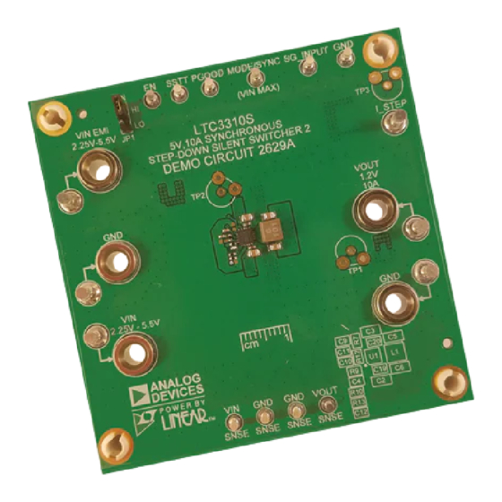
Page 2: Board Photo
DEMO MANUAL DC2629A BOARD PHOTO 1.2V 10A Step-Down Converter 2.25V 0.22 F 0.22 F 22 F 22 F TO 5.5V V IN PGOOD V IN 100nH 249k 100k 1.2V MODE/SYNC 15pF 140k 22 F LTC3310S SSTT 0.033 F 100k AGND... -
Page 3: Emi Test Results
DEMO MANUAL DC2629A EMI TEST RESULTS CISPR25 Conducted EMI Emmisions with Class 5 Peak Limits (Voltage Method) –10 PEAK LIMIT PEAK –20 FREQUENCY (MHz) DC2629A G01 DC2629A DEMO BOARD (WITH VOLTAGE APPLIED TO V EMI INPUT) 3.3V INPUT TO 1.2V OUTPUT AT 7.5A, f... - Page 4 DEMO MANUAL DC2629A QUICK START PROCEDURE Demonstration circuit 2629A is easy to set up and evalu- 5. If Pulse Skip Mode is desired, set PS1 to 0V. Install ate the performance of the LTC3310S. Refer to Figure 1 a 0Ω resistor in the R6 location or short the MODE/ for proper measurement equipment setup and follow the SYNC turret to GND.
-
Page 5: Quick Start Procedure
DEMO MANUAL DC2629A QUICK START PROCEDURE Figure 1. Test setup for the DC2629A Demo Board Figure 2. Technique for Measuring Output Ripple and Step Response Rev. 0... - Page 6 DEMO MANUAL DC2629A QUICK START PROCEDURE SG_INPUT 2V/DIV I_STEP 200mV/DIV 200mV 1.20V 20mV/DIV 20 s/DIV LTC3310S DC2629A TRANSIENT = 3.3V = 1.2V = 2A TO 8A Figure 3. Technique for Measuring Load Step Response Rev. 0...
-
Page 7: Theory Of Operation
Select an operating switching frequency below f SW(MAX) Typically, it is desired to obtain an inductor current of 30% The DC2629A demonstration circuit features the of the maximum LTC3310S operating load, 10A. Use the LTC3310S, a Low Voltage Synchronous Step-Down Silent formulas below to calculate the inductor value to obtain Switcher. -
Page 8: Schematic Diagram
DEMO MANUAL DC2629A SCHEMATIC DIAGRAM Rev. 0... -
Page 9: Parts List
Devices for its use, nor for any infringements of patents or other rights of third parties that may result from its use. Specifications subject to change without notice. No license is granted by implication or otherwise under any patent or patent rights of Analog Devices. - Page 10 Board until you have read and agreed to the Agreement. Your use of the Evaluation Board shall signify your acceptance of the Agreement. This Agreement is made by and between you (“Customer”) and Analog Devices, Inc. (“ADI”), with its principal place of business at One Technology Way, Norwood, MA 02062, USA. Subject to the terms and conditions of the Agreement, ADI hereby grants to Customer a free, limited, personal, temporary, non-exclusive, non-sublicensable, non-transferable license to use the Evaluation Board FOR EVALUATION PURPOSES ONLY.
Need help?
Do you have a question about the DC2629A and is the answer not in the manual?
Questions and answers