Table of Contents
Advertisement
Quick Links
UM1570
User manual
Discovery kit with STM32F303VC MCU
Introduction
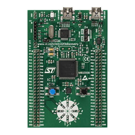
The STM32F3DISCOVERY Discovery kit is a complete demonstration and development
®
®
platform for the STMicroelectronics Arm
Cortex
-M4 core-based STM32F303VCT6
microcontroller. It includes an ST-LINK/V2 (or V2-B) embedded debug tool interface, an ST
MEMS gyroscope, an ST MEMS E-compass, LEDs, push-buttons, and a USB Mini-B
connector.
Figure 1. STM32F3DISCOVERY
Picture is not contractual.
September 2023
UM1570 Rev 7
1/41
www.st.com
1
Advertisement
Table of Contents

Related Manuals for ST STM32F3DISCOVERY


Summary of Contents for ST STM32F3DISCOVERY
-
Page 1: Figure 1. Stm32F3Discovery
® platform for the STMicroelectronics Arm Cortex -M4 core-based STM32F303VCT6 microcontroller. It includes an ST-LINK/V2 (or V2-B) embedded debug tool interface, an ST MEMS gyroscope, an ST MEMS E-compass, LEDs, push-buttons, and a USB Mini-B connector. Figure 1. STM32F3DISCOVERY Picture is not contractual. -
Page 2: Table Of Contents
The STM32F3DISCOVERY Discovery board mechanical drawing ..14 Embedded ST-LINK/V2 (or V2-B) ......15 6.2.1... - Page 3 Extension connectors ........23 STM32F3DISCOVERY information ......34 Product marking .
- Page 4 List of tables UM1570 List of tables Table 1. Ordering information ............7 Table 2.
- Page 5 Figure 5. STM32F3DISCOVERY mechanical drawing ........14 Figure 6.
-
Page 6: Features
STM32F303VCT6 Arm -based microcontroller featuring 256 Kbytes of flash memory, 48 Kbytes of RAM in an LQFP100 package • On-board ST-LINK/V2 for PCB version A or B or ST-LINK/V2-B for PCB version C and newer • USB ST-LINK functions: –... -
Page 7: Ordering Information
Target STM32 STM32F3DISCOVERY MB1035 STM32F303VCT6 1. STM32F3DISCOVERY with ST-LINK/V2 for PCB version B, with ST-LINK/V2-B for PCB version C and newer. 2. Subsequently named main board in the rest of the document. Codification The meaning of the codification is explained in Table Table 2. -
Page 8: Development Environment
The latest versions of the demonstration source code and associated documentation can be downloaded from www.st.com. a. macOS is a trademark of Apple Inc., registered in the U.S. and other countries and regions. -
Page 9: Conventions
UM1570 Conventions Conventions Table 3 defines some conventions used in the present document. Table 3. ON/OFF conventions Convention Definition Jumper JPx ON Jumper fitted Jumper JPx OFF Jumper not fitted Jumper JPx [1-2] Jumper fitted between pin 1 and pin 2 Solder bridge SBx ON SBx connections closed by 0 Ω... -
Page 10: Quick Start
Follow the sequence below to configure the STM32F3DISCOVERY board and launch the DISCOVER application: Check the jumper positions on the board, JP3 ON, CN4 ON (DISCOVERY selected). Connect the STM32F3DISCOVERY board to a PC with a USB cable Type-A or USB ® Type-C to Mini-B through the USB ST-LINK or USB USER connector to power the board. -
Page 11: Hardware Layout And Configuration
The STM32F3DISCOVERY board is designed around the STM32F303VCT6 microcontroller in a 100-pin LQFP package. Figure 2 illustrates the connections between the STM32F303VCT6 and its peripherals (ST-LINK/V2, push-buttons, LEDs, USB, ST MEMS gyroscope, ST MEMS E-compass, and connectors). Figure 2 Figure 3 help the user to locate these features on the STM32F3DISCOVERY board. -
Page 12: Figure 3. Board Layout (Top View)
Hardware layout and configuration UM1570 Figure 3. Board layout (top view) Red/green COM LED (LD2) ST-LINK/V2 USB USER Red PWR LED (LD1) SWD connector (CN3) ST-LINK/ STM32F3DISCOVERY Selector (CN4) measurement LSM303DLHC (JP3) 3 V Power 5 V Power supply supply input/output input/output... -
Page 13: Figure 4. Board Layout (Bottom View)
UM1570 Hardware layout and configuration Figure 4. Board layout (bottom view) SWO (SB10) RESERVED (SB2, SB4, SB6, and SB9) DEFAULT NRST (SB7) (SB1, SB3, SB5, and SB8) STM_RST (SB11) MCO (SB12) RX, TX (SB13) RX, TX (SB15) X3 crystal (SB14) X3 crystal (SB16) X1 crystal (SB17) X1 crystal (SB18) -
Page 14: The Stm32F3Discovery Discovery Board Mechanical Drawing
Hardware layout and configuration UM1570 The STM32F3DISCOVERY Discovery board mechanical drawing Figure 5. STM32F3DISCOVERY mechanical drawing 66.00mm 53.34mm 6.33mm 6.33mm 2.54mm 2.54mm 6.33mm 6.33mm 53.34mm 14/41 UM1570 Rev 7... -
Page 15: Embedded St-Link/V2 (Or V2-B)
Hardware layout and configuration Embedded ST-LINK/V2 (or V2-B) The ST-LINK/V2 on PCB version A or B or the ST-LINK/V2-B on PCB version C is embedded as a programming and debugging tool. Virtual COM port and USB mass storage features are supported by the ST-LINK/V2-B only. -
Page 16: St-Link/V2 (Or V2-B) Firmware Upgrade
The ST-LINK/V2 (or V2-B) embeds a firmware upgrade mechanism for an in-place upgrade through the USB port. The firmware might evolve during the lifetime of the ST-LINK/V2 (or V2-B) product (such as new functionalities, bug fixes, and support for new microcontroller families). -
Page 17: Using St-Link/V2 (Or V2-B) To Program/Debug An External Stm32
Using ST-LINK/V2 (or V2-B) to program/debug an external STM32 application It is very easy to use the ST-LINK/V2 (or V2-B) to program the STM32 on an external application. Remove the two jumpers from CN4 as shown in Figure 8: ST-LINK/V2 (or V2-B) -
Page 18: Figure 8. St-Link/V2 (Or V2-B) Connections
Hardware layout and configuration UM1570 Figure 8. ST-LINK/V2 (or V2-B) connections 18/41 UM1570 Rev 7... -
Page 19: Power Supply And Power Selection
5 V and 3 V can also be used as input power supplies, for example when the USB connectors are not connected to the PC. In this case, the STM32F3DISCOVERY board must be powered by a power supply unit or by auxiliary equipment complying with the standard EN 62368-1:2014+A11:2017 and must be Safety Extra Low Voltage (SELV) with limited power capability. -
Page 20: Usb Device Supported
USB joystick, mouse, or another similar device. If both USBs are connected, diodes D4 and D5 protect the board and use the power from the USB ST-LINK. The board can be powered through this USB USER connector, then LED1 PWR lights and LED2 COM blinks and it can run an application in standalone mode. -
Page 21: Osc Clock
The following information indicates all configurations for clock supply selection: • MCO from ST-LINK. From MCO of the STM32F103C8T6. This frequency cannot be changed. It is fixed at 8 MHz and connected to the PF0-OSC_IN pin of the STM32F303VCT6. Configuration needed: –... -
Page 22: Solder Bridges
B1 push-button is connected to PA0 SB20 (B1-USER) B1 push-button is not connected to PA0 STM32F303VCT6 USART1 is not connected to ST-LINK, so VCP is disabled (Default configuration on PCB version A or B). SB13,15 (RX, TX) STM32F303VCT6 USART1 is connected to ST-LINK, so VCP is enabled (default configuration on PCB version C and newer). -
Page 23: Extension Connectors
Hardware layout and configuration 6.12 Extension connectors The male headers P1 and P2 can connect the STM32F3DISCOVERY to a standard prototyping/wrapping board. STM32F303VCT6 GPIOs are available on these connectors. An oscilloscope, logical analyzer, or voltmeter can also probe P1 and P2. - Page 24 Hardware layout and configuration UM1570 Table 7. STM32F303VCT6 MCU pin description versus board function (continued) MCU pin Board function Main Alternate function function TIM2_CH1_ETR, G2_IO2, SPI1_SCK TIM16_CH1, TIM3_CH1, G2_IO3, TIM8_BKIN, SPI1_MISO, TIM1_BKIN, AOP2_OUT, COMP1_OUT TIM17_CH1, TIM3_CH2, G2_IO4, TIM8_CH1N, SPI1_MOSI, TIM1_CH1N, COMP2_OUT MCO, I2C2_SMBAL, I2S2_MCK,...
- Page 25 UM1570 Hardware layout and configuration Table 7. STM32F303VCT6 MCU pin description versus board function (continued) MCU pin Board function Main Alternate function function TIM17_BKIN, G4_IO2, I2C2_SDA, TIM1_CH3, PA10 USART1_RX, COMP6_OUT, TIM2_CH4, TIM8_BKIN TIM1_CH1N, USART1_CTS, COMP1_OUT, PA11 CAN_RX, TIM4_CH1, TIM1_CH4_BKIN2, USBDM TIM16_CH1, TIM1_CH2N, USART1_RTS,...
- Page 26 Hardware layout and configuration UM1570 Table 7. STM32F303VCT6 MCU pin description versus board function (continued) MCU pin Board function Main Alternate function function JTDI, TIM2_CH1_ETR, TIM8_CH1, I2C1_SCL, PA15 SPI1_NSS, SPI3_NSS/I2S3_WS, USART2_RX, TIM1_BKIN TIM3_CH3, G3_IO2, TIM8_CH2N, TIM1_CH2N TIM3_CH4, G3_IO3, TIM8_CH3N, TIM1_CH3N, COMP4_OUT, AOP3_OUT G3_IO4...
- Page 27 UM1570 Hardware layout and configuration Table 7. STM32F303VCT6 MCU pin description versus board function (continued) MCU pin Board function Main Alternate function function TIM16_BKIN, TIM3_CH2, TIM8_CH3N, I2C1_SMBAL, SPI1_MOSI, SPI3_MOSI/I2S3_D OUT, USART2_CK, TIM17_CH1 TIM16_CH1N, TIM4_CH1, G5_IO3, I2C1_SCL, TIM8_CH1, TIM8_ETR_BKIN2, USART1_TX TIM17_CH1N, TIM4_CH2, G5_IO4, I2C1_SDA, TIM8_BKIN,...
- Page 28 Hardware layout and configuration UM1570 Table 7. STM32F303VCT6 MCU pin description versus board function (continued) MCU pin Board function Main Alternate function function TIM2_CH4, G6_IO1, PB11 USART3_RX, COMP2_OUT G6_IO2, I2C2_SMBAL, SPI2_NSS/I2S2_WS, PB12 TIM1_BKIN, USART3_CK, AOP4_OUT G6_IO3, SPI2_SCK/I2S2_CK, PB13 TIM1_CH1N, USART3_CTS TIM15_CH1, G6_IO4, PB14...
- Page 29 UM1570 Hardware layout and configuration Table 7. STM32F303VCT6 MCU pin description versus board function (continued) MCU pin Board function Main Alternate function function USART1_TX G3_IO1, USART1_RX TIM3_CH1, TIM8_CH1, I2S2_MCK, COMP6_OUT TIM3_CH2, TIM8_CH2, I2S3_MCK, COMP5_OUT TIM3_CH3, TIM8_CH3, COMP3_OUT TIM3_CH4, TIM8_CH4_BKIN2, COMP3_OUT TIM8_CH1N, UART4_TX, PC10...
- Page 30 Hardware layout and configuration UM1570 Table 7. STM32F303VCT6 MCU pin description versus board function (continued) MCU pin Board function Main Alternate function function TIM8_CH3N, UART5_TX, PC12 SPI3_MOSI/ I2S3_DOUT, USART3_CK PC13 TIM1_CH1N PC14 OSC32_IN PC15 OSC32_OUT CAN_RX TIM8_CH4_BKIN2, CAN_TX TIM3_ETR, TIM8_BKIN, UART5__RX TIM2_CH1_ETR, USART2_CTS...
- Page 31 UM1570 Hardware layout and configuration Table 7. STM32F303VCT6 MCU pin description versus board function (continued) MCU pin Board function Main Alternate function function USART3_TX USART3_RX PD10 USART3_CK PD11 USART3_CTS TIM4_CH1, G8_IO1, PD12 USART3_RTS PD13 TIM4_CH2, G8_IO2 PD14 TIM4_CH3, G8_IO3 TIM4_CH4, G8_IO4, PD15 SPI2_NSS TIM4_ETR,...
- Page 32 Hardware layout and configuration UM1570 Table 7. STM32F303VCT6 MCU pin description versus board function (continued) MCU pin Board function Main Alternate function function TRACED3 TIM1_ETR TIM1_CH1N TIM1_CH1 PE10 TIM1_CH2N PE11 TIM1_CH2 PE12 TIM1_CH3N PE13 TIM1_CH3 PE14 TIM1_CH4_BKIN2 TIM1_BKIN, PE15 USART3_RX OSC_IN, I2C2_SDA, TIM1_CH3N OSC_OUT,...
- Page 33 UM1570 Hardware layout and configuration Table 7. STM32F303VCT6 MCU pin description versus board function (continued) MCU pin Board function Main Alternate function function COMP1_OUT TIM4_CH4, I2C2_SCL, USART3_RTS TIM15_CH1, SPI2_SCK TIM15_CH2, PF10 SPI2_SCK 1. The cells marked in gray identify connections between the MCU pin function and the board function. UM1570 Rev 7 33/41...
-
Page 34: Stm32F3Discovery Information
Parts marked as "ES" or "E" are not yet qualified and therefore not approved for use in production. ST is not responsible for any consequences resulting from such use. In no event will ST be liable for the customer using any of these engineering samples in production. -
Page 35: Stm32F3Discovery Product History
UM1570 STM32F3DISCOVERY information STM32F3DISCOVERY product history Table 8. Product history Order Product change Product identification Product details Product limitations code description MCU: – STM32F303VCT6 silicon revision “Y” MCU errata sheet: STM32F3DISCOVER/ Initial revision No limitation – STM32F303xB/C device errata (ES0204) Board: –... -
Page 36: Table 8. Product History
STM32F3DISCOVERY information UM1570 Table 8. Product history (continued) Order Product change Product identification Product details Product limitations code description MCU: – STM32F303VCT6 silicon revision “Y” – Main board revision MCU errata sheet: changed 32F303CDISC1/ No limitation – STM32F303xB/C – Order code STM32F303C-... -
Page 37: Board Revision History
UM1570 STM32F3DISCOVERY information Board revision history Table 9. Board revision history Board variant and Board change Board reference Board limitations revision description Default-B01 Initial revision – PCB label MB1035-C01, SB13 and SB15 ON – STM32F103C8T6 Default-C01 replaced by STM32F103CBT6, ST-... -
Page 38: Federal Communications Commission (Fcc) And Ised Canada (Ic) Compliance Statements
Federal Communications Commission (FCC) and ISED Canada (IC) Compliance Statements Federal Communications Commission (FCC) and ISED Canada (IC) Compliance Statements FCC Compliance Statement Part 15.19 This device complies with part 15 of the FCC Rules. Operation is subject to the following two conditions: (1) this device may not cause harmful interference, and (2) this device must accept any interference received, including interference that may cause undesired operation. -
Page 39: Ised Compliance Statement
UM1570 Federal Communications Commission (FCC) and ISED Canada (IC) Compliance State- ISED Compliance Statement Compliance Statement ISED Canada ICES-003 Compliance Label: CAN ICES-3 (B) / NMB-3 (B). Déclaration de conformité Étiquette de conformité à la NMB-003 d'ISDE Canada: CAN ICES-3 (B) / NMB-3 (B). UM1570 Rev 7 39/41... -
Page 40: Revision History
Figure 12 on page 35 Updated Section 6.2: Embedded ST-LINK/V2 (or V2-B): removed 07-Feb-2013 WLCSP package, sigma-delta ADC, CEC, updated timers and SPI/I²Ss. Updated to introduce the information that boards come with ST- LINK/V2 or ST-LINK/V2-B. Updated Section 1: Features, Section 3: Ordering information, Section 6.2.4: Using ST-LINK/V2 (or V2-B) to program/debug the... - Page 41 ST products and/or to this document at any time without notice. Purchasers should obtain the latest relevant information on ST products before placing orders. ST products are sold pursuant to ST’s terms and conditions of sale in place at the time of order acknowledgment.
Need help?
Do you have a question about the STM32F3DISCOVERY and is the answer not in the manual?
Questions and answers