Table of Contents
Advertisement
Quick Links
SiT6712EB Evaluation Board User Manual
Contents
1 Introduction ............................................................................................................................................. 1
2 I/O Descriptions ....................................................................................................................................... 2
3 EVB Usage Descriptions ........................................................................................................................... 2
3.1 EVB Configurations........................................................................................................................ 2
3.1.1 LVPECL, Standard Termination, Active Probe .................................................................. 3
3.1.2 LVPECL, AC-coupling Configuration, Direct to Instrument ............................................... 3
3.1.3 LVPECL, Y-Termination, Active Probe ............................................................................... 4
3.1.4 LVDS, Standard Termination, Active Probe ...................................................................... 5
3.1.5 LVDS, AC-coupling Configuration, Direct to Instrument .................................................. 5
3.1.6 HCSL, Standard Termination, Active Probe ...................................................................... 6
3.1.7 HCSL, Standard Termination, Direct to Instrument ......................................................... 6
2
C and SPI Interfaces .................................................................................................................... 7
3.3 Waveform Measurement Using Active Probe .............................................................................. 7
3.4 Jitter Measurement ...................................................................................................................... 8
Appendix A - Schematic, BOM and Layout of SiT6712EB ............................................................................. 9
1
Introduction
The SiT6712EB evaluation board (EVB) is designed for use with SiTime's In-system programmable
oscillators (ISP-DCXO) that support the differential signaling outputs in the 5.0x3.2 mm 10-pin QFN
package. It enables the user to evaluate all aspects of the ISP-DCXO devices including signal integrity,
phase noise, phase jitter and the re-programming of the output frequency via I
EVB Features
-
Support for SiT3521 (1 to 340 MHz) and SiT3522 (340.000001 to 725 MHz) ISP-DCXOs
-
Probing points for output frequency measurements
o Support for LVPECL, LVDS and HCSL output signal types
o Support for waveform measurements
o Support for phase noise and phase jitter measurements
-
Connector access to I
-
Connector access for current consumption measurements
SiTime typically ships the EVB pre-configured with the ISP-DCXO device specified by the user. The end
user can re-configure the EVB for an ISP-DCXO device of a different configuration.
SiT6712EB UM Rev 1.02
2
C and/or SPI interfaces
Page 1 of 13
2
C/SPI interfaces.
www.sitime.com
Advertisement
Table of Contents

Related Manuals for SiTime SiT6712EB


Summary of Contents for SiTime SiT6712EB
-
Page 1: Table Of Contents
C and/or SPI interfaces Connector access for current consumption measurements SiTime typically ships the EVB pre-configured with the ISP-DCXO device specified by the user. The end user can re-configure the EVB for an ISP-DCXO device of a different configuration. SiT6712EB UM Rev 1.02 Page 1 of 13 www.sitime.com... -
Page 2: O Descriptions
Note: Pin 1 location of the ISP-DCXO device on EVB is indicated by a chamfer in the silkscreen pattern around the device footprint. EVB Usage Descriptions EVB Configurations The SiT6712EB supports multiple configurations for different signaling types of SiTime differential oscillators by using different component loading options. Refer to Figure A1 in Appendix A for the SiT6712EB schematics Figure A2 in Appendix A for the SiT6712EB layout top view SiT6712EB UM Rev 1.02... -
Page 3: Lvpecl, Standard Termination, Active Probe
Any components without assigned nominal values are populated only for specific configuration of EVB where these parts are needed Any components labeled “DNP” are not populated on the EVB and are reserved for SiTime internal use only 3.1.1 LVPECL, Standard Termination, Active Probe In this configuration, the LVPECL outputs are terminated to Vbias = VDD –... -
Page 4: Lvpecl, Y-Termination, Active Probe
SiT6712EB Evaluation Board User Manual Figure 2: LVPECL output termination with 150 Ω/120 Ω to GND and measurement with AC-coupled connection to measurement instrument using 50 Ω SMA cables 3.1.3 LVPECL, Y-Termination, Active Probe This configuration is intended for LVPECL output waveform parameters measurement using active probe. -
Page 5: Lvds, Standard Termination, Active Probe
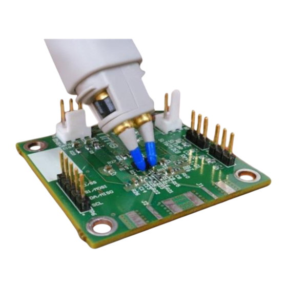
SiT6712EB Evaluation Board User Manual 3.1.4 LVDS, Standard Termination, Active Probe This configuration is intended for LVDS output waveform parameters measurement using active probe. A high-speed active probe, as shown on Figure 4 is placed on the termination resistor’s pads which are on the OUT+ and OUT- traces. -
Page 6: Hcsl, Standard Termination, Active Probe
SiT6712EB Evaluation Board User Manual 3.1.6 HCSL, Standard Termination, Active Probe This configuration is intended for HCSL output waveform parameters measurement using active probe. Output is terminated with 50 Ω (R12 and R25) to GND. Series resistors R15 and R22 are used as overshoot limiter and should be in range from 10 Ω... -
Page 7: I 2 C And Spi Interfaces
C or the SPI support per user specification. Waveform Measurement Using Active Probe SiTime differential oscillators are high speed logic output devices with fast, sub-nanosecond rise/fall time. It is critical that the proper logic and high frequency measurement techniques are used along with the high-quality active probe to ensure best measurement results. -
Page 8: Jitter Measurement
SiT6712EB EVB Jitter Measurement For jitter measurement, configurations described in 3.1.1 (LVPECL), 3.1.4 (LVDS) and 3.1.6 (HCSL) should be used. Jitter measurement technique is described in SiTime application note AN10007. SiT6712EB UM Rev 1.02 Page 8 of 13... -
Page 9: Appendix A - Schematic, Bom And Layout Of Sit6712Eb
SiT6712EB Evaluation Board User Manual Appendix A – Schematic, BOM and Layout of SiT6712EB Place away from P1 and P4 10uH Vdd_sense 10uF 0.1uF Pin2 Place close to DUT VDD pin "curr_meas_inp" 10uF "curr_meas_out" DUT_GND DUT_GND Vbias Pin1 Place close to DUT pin1... - Page 10 SiT6712EB Evaluation Board User Manual Table A1: Bill of Materials (BOM) Reference Designators Description SMD component size Value R1, R19 Resistor 0603 0 Ω R14, R28 Resistor 0402 0 Ω R2, R9, Resistor 0603 10 Ω R5, R6 Resistor 0603 51 Ω...
- Page 11 SiT6712EB Evaluation Board User Manual Ceramic capacitor 0603 Don’t populated C10, C11 Ceramic capacitor 0402 Don’t populated SiTime Oscillator P1, P5 3-pin connector Through hole, 2.54 mm pitch P2, P3 3-pin header Through hole, 2.54 mm pitch 5-pin header Through hole, 2.54...
- Page 12 SiT6712EB Evaluation Board User Manual Probe test points Figure A2: SiT6712EB rev.2.01 layout SiT6712EB UM Rev 1.02 Page 12 of 13 www.sitime.com...
- Page 13 © SiTime Corporation, January 2023. The information contained herein is subject to change at any time without notice. SiTime assumes no responsibility or liability for any loss, damage or defect of a Product which is caused in whole or in part by (i) use of any circuitry other than circuitry embodied in a SiTime product, (ii) misuse or abuse including static discharge, neglect or accident, (iii) unauthorized modification or repairs which have been soldered or altered during assembly and are not capable of being tested by SiTime under its normal test conditions, or (iv) improper installation, storage, handling, warehousing or transportation, or (v) being subjected to unusual physical, thermal, or electrical stress.
Need help?
Do you have a question about the SiT6712EB and is the answer not in the manual?
Questions and answers