Advertisement
DESCRIPTION
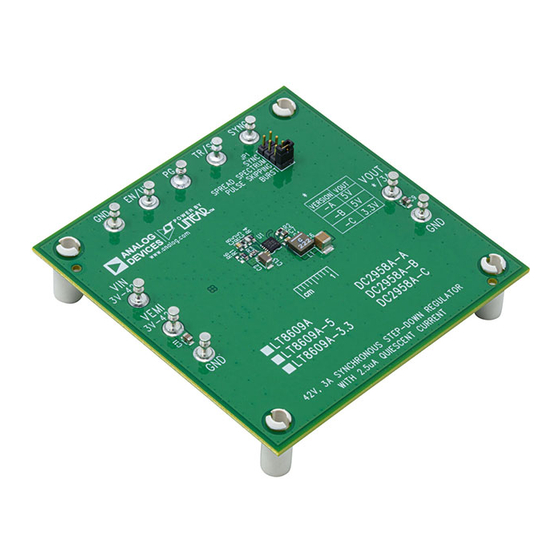
Demonstration circuit 2958A is a 42V, 3A micro-
power synchronous step-down regulator featuring the
LT
8609A/09A-5/09A-3.3. There are three assembly ver-
®
sions; DC2958A-A is for the LT8609A adjustable output,
DC2958A-B is for the LT8609A-5 with a fixed 5V output
voltage and DC2958A-C is for the LT8609A-3.3 with a
fixed 3.3V output voltage.
The LT8609A/09A-5/09A-3.3 is a compact, high efficiency,
high speed synchronous monolithic step-down switching
regulator that consumes only 2.5μA of quiescent current.
Top and bottom power switches, compensation compo-
nents and other necessary circuits are inside of the IC to
minimize external components and simplify design.
The SYNC pin on the demo board is grounded by default
for low ripple Burst Mode operation. Moving JP1 to
PULSE SKIPPING position changes the operation mode to
pulse-skipping operation. Once JP1 is placed on SPREAD
SPECTRUM position, V
CC
low EMI spread spectrum operation. To synchronous to
an external clock, move JP1 to SYNC and apply the exter-
nal clock to the SYNC turret.
The demo board is designed for 5V or 3.3V output with
up to 42V input. The wide input range allows a variety of
input sources, such as automotive batteries and industrial
supplies. The minimum input voltage can be as low as 3V
PERFORMANCE SUMMARY
SYMBOL
PARAMETER
V
Input Voltage Range
IN
V
Output Voltage
OUT
I
Maximum Output Current
OUT
f
Switching Frequency
SW
Efficiency for DC2958A-A/DC2958A-B
EFF
Efficiency for DC2958A-C
42V, 3A Micropower Synchronous
is applied to the SYNC pin for
Specifications are at T
CONDITIONS
DC2958A-A/DC2958A-B
DC2958A-C
V
= 12V, I
IN
OUT
V
= 12V, I
IN
OUT
DEMO MANUAL DC2958A
LT8609A/09A-5/09A-3.3
Step-Down Regulator
for drop out mode operation. Under this mode, the output
voltage is below the regulation point and follow the input
voltage. To maintain the output under regulation, input
voltage should be above certain value. For DC2958A-A
(adjustable) and DC2958A-B (5V), this value is 5.5V
while 3.8V for DC2958A-C (3.3V). The rated maximum
load current is 3A, while derating is necessary for certain
input voltage and thermal conditions. Figure 1 shows the
efficiency of the circuit. Figure 2 shows the IC top tem-
perature rising on DC2958A demo board under different
load conditions.
The demo board has an EMI filter installed. The radiated
EMI performances of the board (with EMI filter) are shown
in Figure 3 and Figure 4. The red lines in Figure 3 and
Figure 4 are CISPR25 Class 5 peak limit. To use the EMI
filter, the input should be tied to V
L2, which is shorted on the board by default, can be added
in the EMI filter to further reduce the conducted emission.
The LT8609A/09A-5/09A-3.3 data sheet gives a complete
description of the part, operation and application informa-
tion. The data sheet must be read in conjunction with this
demo manual for DC2958A.
Design files for this circuit board are
All registered trademarks and trademarks are the property of their respective owners.
= 25°C
A
MIN
4.8
3.168
3
1.85
= 1A
= 1A
, not V
. An inductor
EMI
IN
available.
TYP
MAX
42
5
5.2
3.3
3.432
2
2.15
92.1
89.3
UNITS
V
V
A
MHz
%
%
Rev. 0
1
Advertisement
Table of Contents

Subscribe to Our Youtube Channel
Related Manuals for Analog Devices DC2958A


Summary of Contents for Analog Devices DC2958A
- Page 1 DC2958A-A is for the LT8609A adjustable output, voltage should be above certain value. For DC2958A-A DC2958A-B is for the LT8609A-5 with a fixed 5V output (adjustable) and DC2958A-B (5V), this value is 5.5V voltage and DC2958A-C is for the LT8609A-3.3 with a while 3.8V for DC2958A-C (3.3V).
- Page 2 DEMO MANUAL DC2958A QUICK START PROCEDURE = 12V LT8609A-5 LT8609A-3.3 LOAD CURRENT (A) DC2958 F01 Figure 1. Efficiency vs Load Current at 12V Input 2MHz Switching Frequency LT8609A-5 LT8609A-3.3 12V LT8609A-5 LT8609A-3.3 24V LOAD CURRENT (A) DC2958A F02 Figure 2. LT8609A Demo Circuit Case Temperature Rise...
- Page 3 SPREAD SPECTRUM MODE FIXED FREQUENCY –20 1000 FREQUENCY (MHz) DC2958A–A/ DC2958A–B DEMO BOARD DC2958 F03 (WITH EMI FILTER INSTALLED) 14V INPUT TO 5V OUTPUT AT 2A, f = 2MHz Figure 3. LT8609A-5 Demo Circuit EMI Performance in CISPR25 Radiated Emission Test,...
- Page 4 DEMO MANUAL DC2958A QUICK START PROCEDURE DC2958A is easy to set up to evaluate the performance of 5. Once the proper output voltage is established, connect the LT8609A/09A-5/LT8609A/09A-3.3. Refer to Figure 5 a variable load capable of sinking 3A to the output ter-...
- Page 5 DEMO MANUAL DC2958A QUICK START PROCEDURE Figure 5. Proper Measurement Equipment Setup Figure 6. Measuring Output Ripple Rev. 0...
- Page 6 COILCRAFT, XFL4020-222MEC RES., CHIP , 18.2k, 1/10W, 1%, 0603 VISHAY, CRCW060318K2FKEA RES., CHIP , 49.9k, 1/10W, 1%, 0603 VISHAY, CRCW060349K9FKEA DC2958A-A Version Specific Components IC, REGULATOR, DDM-10 ANALOG DEVICES, LT8609AEDDM#PBF CAP ., C0G, 10pF, 25V, 5%, 0603 AVX, 06033A100JAT2A RES., CHIP , 1MΩ, 1/10W, 1%, 0603 VISHAY, CRCW06031M00FKEA RES., CHIP , 187k, 1/10W, 1%, 0603...
- Page 7 Devices for its use, nor for any infringements of patents or other rights of third parties that may result from its use. Specifications subject to change without notice. No license is granted by implication or otherwise under any patent or patent rights of Analog Devices.
- Page 8 Board until you have read and agreed to the Agreement. Your use of the Evaluation Board shall signify your acceptance of the Agreement. This Agreement is made by and between you (“Customer”) and Analog Devices, Inc. (“ADI”), with its principal place of business at One Technology Way, Norwood, MA 02062, USA. Subject to the terms and conditions of the Agreement, ADI hereby grants to Customer a free, limited, personal, temporary, non-exclusive, non-sublicensable, non-transferable license to use the Evaluation Board FOR EVALUATION PURPOSES ONLY.
Need help?
Do you have a question about the DC2958A and is the answer not in the manual?
Questions and answers