Table of Contents
Advertisement
Quick Links
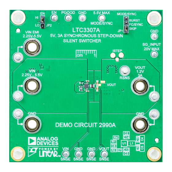
DESCRIPTION
Demonstration circuit 2990A features the
5V, 3A synchronous step-down Silent Switcher
ating as a 2MHz, 3.3V to 1.2V 3A buck regulator. The
LTC3307A supports adjustable output voltages from
0.5V to V
with operating frequencies from 1MHz up to
IN
3MHz. The LTC3307A is a compact, ultralow emission,
high efficiency, and high speed synchronous monolithic
step-down switching regulator. A minimum on-time of
22ns enables high V
to low V
IN
high frequencies.
The DC2990A operating mode may be selected as Burst,
Skip or forced continuous (FC) mode. Setting JP1 to the
FC/SYNC position will allow the LTC3307A to sync to
a clock frequency from 1MHz to 3MHz. The LTC3307A
operates in forced continuous mode when syncing to an
external clock. The DC2990A is set to a fixed 2MHz fre-
quency by connecting RT to V
The frequency can be easily changed by removing R9 and
setting an appropriate resistor in the R4 location to obtain
the desired frequency. Refer to the LTC3307A data sheet
for the proper RT value for a desired switching frequency.
PERFORMANCE SUMMARY
SYMBOL
PARAMETER
V
Input Voltage Range
IN
V
V
Voltage Range*
OUT
OUT
I
Output Current
OUT
f
Switching Frequency
SW
T
Top Switch Minimum On-Time
ON
Duty Cycle
Top Switch Duty Cycle
*With 1% resistors. Accuracy will improve to within 1% using 0.1% resistors.
5V Input to 1.2V Output at 3A Synchronous
Step‑Down Silent Switcher Demo Circuit
LTC
3307A
®
®
conversion ratios at
OUT
through a 0Ω resistor, R9.
IN
Specifications are at T
CONDITIONS
V
IN
DEMO MANUAL DC2990A
The DC2990A also has an EMI filter to reduce conducted
oper-
EMI. This EMI filter can be included by applying the input
voltage at the V
IN
the board is shown in the EMI Test Results section. The
red lines in the EMI performance graphs illustrate the
CISPR25 Class 5 peak limits for the conducted and radi-
ated emission tests.
The LTC3307A data sheet gives a complete description
of the device, operation and application information. The
data sheet must be read in conjunction with this demo
manual. The LTC3307A is assembled in a 2mm × 2mm
LQFN package with exposed pads for low thermal resis-
tance. The layout recommendations for low EMI operation
and maximum thermal performance are available in the
data sheet section Low EMI PCB Layout.
The Efficiency vs Load graph shows the efficiency and
the power loss of the circuit with a 3.3V input in Burst
Mode operation.
Design files for this circuit board are
All registered trademarks and trademarks are the property of their respective owners.
= 25°C
A
Greater than V
OUT
LTC3307A
EMI terminal. The EMI performance of
available.
MIN
TYP
MAX
2.25
1.183
1.2
1.217
1
22
UNITS
5.5
V
V
3
A
3
MHz
ns
100
%
Rev. 0
1
Advertisement
Table of Contents

Subscribe to Our Youtube Channel
Related Manuals for Analog Devices DC2990A


Summary of Contents for Analog Devices DC2990A
- Page 1 Low EMI PCB Layout. external clock. The DC2990A is set to a fixed 2MHz fre- The Efficiency vs Load graph shows the efficiency and quency by connecting RT to V through a 0Ω...
-
Page 2: Board Photo
DEMO MANUAL DC2990A BOARD PHOTO CIRCUIT SCHEMATIC High Efficiency, 2MHz, 1.2V 3A Step-Down Converter Efficiency and Power Loss in Burst Mode Operation = 2.25V TO 5.5V 1µF 1µF 4.7µF 4.7µF EFFICIENCY 0201 0201 470nH 1.2V 10pF 140k 15µF LTC3307A 0.01... -
Page 3: Emi Test Results
DEMO MANUAL DC2990A EMI TEST RESULTS Conducted EMI Performance (CISPR25 Conducted Emission Test with Class 5 Peak Limits) CLASS 5 PEAK LIMIT –10 MEASURED EMISSIONS RADIATED NOISE –20 FREQUENCY (MHz) DC2990A DEMO BOARD dc2990a G01 (WITH EMI FILTER INSTALLED) 3.3V INPUT TO 1.2V OUTPUT AT 2.4A, f... - Page 4 DEMO MANUAL DC2990A QUICK START PROCEDURE Demonstration circuit 2990A is easy to set up and evalu- 9. Set the load current to 0.2A and repeat Step 8. Observe ate the performance of the LTC3307A. Refer to Figure 1 that the switching waveform is now operating in pulse- for proper measurement equipment setup and follow the skippping mode.
-
Page 5: Quick Start Procedure
DEMO MANUAL DC2990A QUICK START PROCEDURE Figure 1. Test Setup for the DC2990A Demo Board Figure 2. Technique for Measuring Output Ripple Figure 3. Technique for Measuring Output Ripple and Step and Step Response with a Scope Probe Response with a Low Inductance Connector (Not Supplied) -
Page 6: Theory Of Operation
THEORY OF OPERATION Introduction to the DC2990A the external clock while operating in forced continuous The DC2990A features the LTC3307A, a low voltage syn- mode. See the LTC3307A data sheet for more detailed chronous step-down Silent Switcher. The LTC3307A is a information. - Page 7 DEMO MANUAL DC2990A THEORY OF OPERATION Accurately Measuring Output Ripple of the LTC3307A to the output capacitors as close to the inductor as pos- sible. Adding capacitors close to the load creates a π filter With the fast edge rates of the circuit, high frequency...
-
Page 8: Parts List
DEMO MANUAL DC2990A PARTS LIST ITEM REFERENCE PART DESCRIPTION MANUFACTURER/PART NUMBER Required Circuit Components CAP ., 0.01μF, X7R, 10V, 10%, 0201 MURATA, GRM033R70J103KA01D C2, C3 CAP ., 4.7μF, X6S, 6.3V, 20%, 0402 MURATA, GRM155C80J475MEAAD C4, C5 CAP ., 22μF, X6S, 6.3V, 20%, 0603 MURATA, GRM188C80J226ME15D CAP ., 10pF, C0G, 50V, 5%, 0402, AEC-Q200... -
Page 9: Schematic Diagram
Devices for its use, nor for any infringements of patents or other rights of third parties that may result from its use. Specifications subject to change without notice. No license is granted by implication or otherwise under any patent or patent rights of Analog Devices. - Page 10 By using the evaluation board discussed herein (together with any tools, components documentation or support materials, the Evaluation Board”), you are agreeing to be bound by the terms and conditions set forth below (Agreement”) unless you have purchased the Evaluation Board, in which case the Analog Devices Standard Terms and Conditions of Sale shall govern. Do not use the Evaluation Board until you have read and agreed to the Agreement.
Need help?
Do you have a question about the DC2990A and is the answer not in the manual?
Questions and answers