Table of Contents
Advertisement
Quick Links
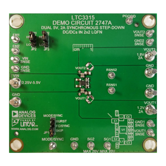
DESCRIPTION
Demonstration Circuit DC2747A features the
dual 5V, 2A Synchronous Step-Down DC/DC regulators
operating at 2.0MHz. One regulator provides a 1.2V out-
put and the other provides 1.8V, both up to a 2A load. The
LTC3315A supports adjustable output voltages from 0.5V
to V
, operating frequencies from 1MHz up to 3MHz. The
IN
LTC3315A is a compact, high efficiency, and high speed
synchronous monolithic step-down switching regulator.
Fast minimum on-time of 25ns enables high V
V
conversion at high frequency.
OUT
The DC2747A operating mode may be selected as Burst
Mode operation, Skip mode or Forced Continuous (FC)
mode. Setting JP1 to the FC/SYNC position will allow
the LTC3315A to sync to a clock frequency from 1MHz
PERFORMANCE SUMMARY
PARAMETER
Input Supply Range (V
)
IN
Internal Oscillator Frequency (f
SW
Top Switch On Time
V
OUT1
V
OUT2
V
IN
2.25V TO 5.5V
10µF
10µF
Dual 5V, 2A Synchronous Step-Down
LTC
©
IN
Specifications are at T
CONDITIONS
)
0 to 2A
0 to 2A
680nH
V
SW1
IN
1µF
FB1
EN1
LTC3315A
V
IN
1µH
SW2
1µF
EN2
FB2
MODE/SYNC
1M
PGOOD
GND
f
= 2MHz
DC2747 F01
SW
DEMO MANUAL DC2747A
DC/DCs in 2mm × 2mm LQFN
3315A
to 3MHz. The LTC3315A operates in Forced Continuous
mode when syncing to an external clock.
The LTC3315A data sheet gives a complete description
of the device, operation and application information. The
data sheet must be read in conjunction with this demo.
The LTC3315A is assembled in a 2mm × 2mm LQFN pack-
age with exposed pads for low thermal resistance. The
PCB Considerations section in the data sheet.
to low
The Efficiency vs Load graph shows the efficiency and
the power loss of the circuit with a 3.3V input in Burst
Mode operation.
Design files for this circuit board are
All registered trademarks and trademarks are the property of their respective owners.
= 25°C
A
MIN
2.25
1.9
V
OUT1
1.2V, 2A
6.8pF
140k
33µF
100k
V
OUT2
1.8V, 2A
6.8pF
261k
33µF
100k
V
IN
LTC3315A
available.
TYP
MAX
5.5
2
2.1
25
1.2
1.8
95
90
85
80
75
70
0.00
0.25
0.50 0.75
1.00
1.25 1.50 1.75 2.00
I
(A)
OUT
UNITS
V
MHz
ns
V
V
1.2 V
OUT
1.8 V
OUT
DC2747 F02
Rev. 0
1
Advertisement
Table of Contents

Related Manuals for Analog Devices DC2747A


Summary of Contents for Analog Devices DC2747A
- Page 1 The Efficiency vs Load graph shows the efficiency and conversion at high frequency. the power loss of the circuit with a 3.3V input in Burst The DC2747A operating mode may be selected as Burst Mode operation. Mode operation, Skip mode or Forced Continuous (FC) Design files for this circuit board are available.
-
Page 2: Board Photo
DEMO MANUAL DC2747A BOARD PHOTO BOARD PERFORMANCE LTC3315A 1.2V FC MODE LTC3315A 1.8V FC MODE LOAD REGULATION LOAD REGULATION = 3.3V = 3.3V 1.210 1.210 1.205 1.805 1.200 1.800 1.195 1.795 1.190 1.790 2.00 2.00 DC2747 F03 DC2747 F04 Rev. 0... - Page 3 DEMO MANUAL DC2747A BOARD PERFORMANCE 1.2V Load Transient Response Forced Continuous Mode 2V/DIV OUT1 20mV/DIV RSNS1 50mV/DIV 2747A F05 10µs/DIV 3.3V TO 1.2V LOADSTEP 0.4A TO 1.6A 1A/µs 1.8V Load Transient Forced Continuous ModeMode 2V/DIV OUT2 50mV/DIV RSNS2 50mV/DIV 2747A F06 10µs/DIV...
- Page 4 DEMO MANUAL DC2747A QUICK START PROCEDURE The DC2747A is easy to set up to evaluate the perfor- 9. Turn on LOAD2 and slowly increase the from 0A to 2A mance of the LTC3315A. Refer to Figure 1 and Figure 2 and observe the output voltage.
-
Page 5: Quick Start Procedure
DEMO MANUAL DC2747A QUICK START PROCEDURE LOAD2 0A-2A 2.25V-5.5V LOAD1 0A-2A O-SCOPE DC2747A Figure 1. Proper Measurement Equipment Setup Figure 2. Measuring Input or Output Ripple Rev. 0... -
Page 6: Theory Of Operation
Introduction to the DC2747A The maximum allowable operating frequency is influenced by the minimum on time of the top switch, the ratio of V The DC2747A demonstration circuit features the to V and the available inductor values. The maximum LTC3315A, a 5V Dual 2A Low voltage Synchronous Step- allowable operating frequency may be calculated using a Down regulator. - Page 7 3-terminal capacitor with the self-resonant frequency close to the high frequency spikes. Below is the output The DC2747A uses 3-terminal capacitors, C9 and C10, ripple using a 500MHz scope, 50Ω probe measured at on the output to reduce the high frequency spikes that TP1 on without the 3-terminal capacitor populated in C9.
-
Page 8: Parts List
DEMO MANUAL DC2747A PARTS LIST ITEM REFERENCE PART DESCRIPTION MANUFACTURER/PART NUMBER Required Circuit Components C1, C2 CAP ., 10µF, X5R, 10V, 10%, 0603 SAMSUNG, CL10A106KP8NNNC C3, C4 CAP ., 33µF, X5R, 10V, 20%, 0805 TDK, C2012X5R1A336M125AC C5, C6 CAP ., 6.8pF, C0G/NP0, 50V, ±0.5pF, 0402... -
Page 9: Schematic Diagram
Devices for its use, nor for any infringements of patents or other rights of third parties that may result from its use. Specifications subject to change without notice. No license is granted by implication or otherwise under any patent or patent rights of Analog Devices. - Page 10 Board until you have read and agreed to the Agreement. Your use of the Evaluation Board shall signify your acceptance of the Agreement. This Agreement is made by and between you (“Customer”) and Analog Devices, Inc. (“ADI”), with its principal place of business at One Technology Way, Norwood, MA 02062, USA. Subject to the terms and conditions of the Agreement, ADI hereby grants to Customer a free, limited, personal, temporary, non-exclusive, non-sublicensable, non-transferable license to use the Evaluation Board FOR EVALUATION PURPOSES ONLY.
Need help?
Do you have a question about the DC2747A and is the answer not in the manual?
Questions and answers