Table of Contents
Advertisement
Quick Links
1.
2.
2.1 WT-SOM6ULX diagram and shematic .................................................................................................3
2.2 WT-SOM6ULX power management .....................................................................................................4
2.3 i.MX6ULL related power supply domain's ripple test ....................................................................4
3.
3.1 Core boards power on sequence and typical supply circuit ....................................................5
3.2 About reset ....................................................................................................................................................6
3.3 ON/OFF and wakeup .................................................................................................................................7
4. Startup related circuit design ....................................................................................................................7
4.1 Startup mode and stardup device .........................................................................................................7
4.2 Other startup related hardware notice .......................................................................................... 10
5.
6.
7.
7.1 Resistive TP circuit ..................................................................................................................................... 13
7.2 Capacitive TP .............................................................................................................................................. 13
8.
................................................................................................................................................ 14
9.
............................................................................................................................................. 15
10.
11.
................................................................................................................................................... 19
12.
....................................................................................................................................... 20
13.
................................................................................................................................................. 21
14.
............................................................................................................................................................. 21
15.
.................................................................................................................................................................. 21
16.
..................................................................................................................................................... 22
17.
Content
...................................................................................................1
............................................................................................................. 10
........................................................................................................................... 11
...................................................................................................... 12
................................................................................................................................. 16
........................................................................................................................... 23
...........................................................3
1
..........................................5
Advertisement
Table of Contents

Subscribe to Our Youtube Channel
Related Manuals for NXP Semiconductors i.MX6ULL


Summary of Contents for NXP Semiconductors i.MX6ULL
-
Page 1: Table Of Contents
WT-SOM6ULX schematic and testing description ............3 2.1 WT-SOM6ULX diagram and shematic ....................3 2.2 WT-SOM6ULX power management .....................4 2.3 i.MX6ULL related power supply domain’s ripple test ..............4 Based WT-SOM6ULX’s baseboard power system design 3. ..........5 3.1 Core boards power on sequence and typical supply circuit ............5 3.2 About reset ..............................6... - Page 2 ADC interface ............................23...
-
Page 3: 1.Nxp I.mx6Ull Chip Introduction
1.NXP i.MX6ULL chip introduction i.MX6ULL is designed by NXP, high efficiency, cost effective application processor. With advanced implementations of single core ARM Cortex-A7 running up to 900MHz. i.MX 6ULL application processor includes an integrated power management module that reduce the complexity of the external power supply and simplifies power-up sequencing. - Page 4 Pin-to-Pin compatible chip and difference comparison i.MX6ULL BGA289 package main chipset’s part number and parameter comparison list: MCIMX6Y2CVM05AA MCIMX6Y2CVM08AB MCIMX6Y2DVM09AB Parts i.MX 32-bit MPU, i.MX 32-bit MPU, i.MX 32-bit MPU, Marketing ARM Cortex-A7 core, ARM Cortex-A7 core, ARM Cortex-A7 core,...
-
Page 5: Wt-Som6Ulx Schematic And Testing Description
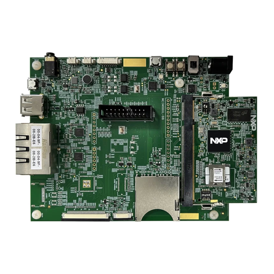
(℃) Camera Interfaces Audio Specific SPDIF Modules WT-SOM6ULX supports i.MX6UltraLite and i.MX6ULL all BGA289 part numbers. Main production model is i.MX6ULL series MCIMX6Y2CVM08AB, Other models produced by order. 2. WT-SOM6ULX schematic and test instruction 2.1 WT-SOM6ULX core board block diagram and schematic For most applications, WT-SOM6ULX designed the smallest system Power Management + DDR3L + NAND/EMMC+ LAN8720(Ethernet Phy). -
Page 6: Wt-Som6Ulx Power Management
2.2 WT-SOM6ULX core board’s power management According to i.MX6ULL power supply timing requirement, core board layout 4 power supply pins: VSNVS,VSYS_3V3,USB_OTG2_VBUS,USB_OTG1_VBUS. VSNVS have to powered first, backup battery power can be used for button ON/OFF switch control, low power consumption, maintenance internal RTC power supply after shutdown, only consume 26uA. -
Page 7: 3. Based Wt-Som6Ulx's Baseboard Power System Design
For all IO pins, ensure that there is no high level input before VSYS_3V3 is powered The above is the power-on timing requirements of the NXP i.MX6ULL chip to ensure long-term stable operation of the whole circuit board. If the timing requirements are violated, the power-on behavior of the chip may be affected, resulting in a small probability of chip damage or startup failure. -
Page 8: About Reset
WT-SOM6ULX typical power supply scheme Power/GND pin Pin number Description VSNVS Have to be powered on first, and have to be powered on when switch power management is required. Main power supply. Power supply is enabled via VSYS_3V3 PMIC_ON_REQ. It is recommended that the string power supply use a magnetic bead (such as 120R 3A) and then place a 2x22uF ceramic capacitor near the pin to form an LC filter. -
Page 9: On/Off And Wakeup
3.3 Switch and wake up i.MX6ULL chip provides the switch of power management function. It is connected to the touch button through the ONOFF pin. When the VSNVS is powered, press about six seconds to pull low the ONOFF. The PMIC_ON_REQ will be pulled low through the above circuit. - Page 10 u-boot, zImage, dtb, rootfs, etc. through the Mfgtools programming tool (installed on Windows system) provided by NXP official website. When BOOT_MODE[1:0] is 10, the i.MX6ULx chip samples the level of LCD_DATA[23:0] during power-on reset to determine the startup device and parameters. The specific description is as follow: The relationship between the level of LCD_DATA[23:0] during power-on and the internal boot eFuse register is as follows:...
- Page 11 Note: When the boot device specified by FUSE does not have a boot program available (such as DCD command), i.MX6ULL will first jump to the MMC/SD1 device boot mode, try to boot from the SD/TF card, if no boot program is available, then finally enter "Serial Downloader"...
-
Page 12: Other Startup Related Hardware Notice
SD/TF card, or connected to SDIO interface module (such as WIFI module). The i.MX6ULL MMC/SD clock is up to 208MHz. In the design, the SDIO bus series matching resistor (usually 22R, placed close to the core board pin) must be used for the same length processing. -
Page 13: 6.Lcd Interface Circuit
LCD_DATA16 SD2_DATA7 NAND_DATA07 CSI_DATA07 LCD_DATA17 6.LCD interface circuit i.MX6ULL LCD interface characteristics: ⚫ LCDIF supports one parallel 24-bit LCD display with up to WXGA (1366 x 768) ⚫ resolution at 60 Hz ⚫ 8/16/18/24/32 bit LCD data bus support available depending on I/O mux options. -
Page 14: 7.Touch Screen Interface Circuit
The length of the line is equal, and the relative length error is <=400mil 7.Touch screen interface circuit i.MX6ULL built in ADC controller, support 4-wire resistive touch screen. At the same time, the capacitive touch screen is supported through the I2C/USB interface. -
Page 15: Resistive Tp Circuit
Resistance TP definition GPIO1_IO04 GPIO1_IO03 GPIO1_IO02 GPIO1_IO01 Resistance TP use and connection mode reference: Resistance TP structure diagram i.MX6ULL connect 4-wire resistance TP schematic 7.2 capacitance TP A common capacitor TP circuit diagram based on I2C interface is as follows:... -
Page 16: Iic Interface
Among them, the RST (reset pin) and INT (interrupt pin) of the capacitor TP can be configured as any pin with GPIO function. 8. IIC interface i.MX6ULL provides up to 4 I2C interfaces. It can be flexibly allocated through pin multiplexing. I2C1 signal reusable list... -
Page 17: Usb Interface
LCD_DATA2 UART2_RX_DATA 9. USB interface i.MX6ULL have 2 way USB 2.0 controller. Each USB OTG controller core can operate in High Speed operation (480 Mbps), Full Speed operation (12 Mbps) and Low Speed operation (1.5 Mbps). 2 way USB related pin... -
Page 18: Ethernet Interface
When more than 2 USB Hosts are required, they are generally extended by a USB Hub chip (such as USB2514). 10. Ethernet interface i.MX6ULL implements a dual-speed 10/100-Mbit/s Ethernet MAC compliant with the IEEE802.3-2002 standard. The MAC layer provides compatibility with half- or full duplex 10/100-Mbit/s Ethernet LANs. - Page 19 ETH1X_LED1 Lan8720A Link activity LED Active High ETH1X_LED2 LAN8720A Speed LED(100M or 10Mbps) Active Low ENET1 connect RJ45 reference schematic as below: ENET1 connect RJ45 schematic When there is a dual network port requirement, the ENET2 can be extended by connecting the LAN8720A through the ENET2 RMII interface.
- Page 20 WT-SOM6ULX module Precautions: 1. The SMI serial bus ENET_MDC, ENET_MDIO is not configurable for other functions unless the core board LAN8720A is not installed. ENET_MDIO has been pulled up from 1.5K ohms to 3.3V on the core board. 2. ENET1 and ENET2 share the same set of SMI serial bus (ENET_MDC, ENET_MDIO), so the two PHY chips must be configured with different PHY addresses.
-
Page 21: Serial Port
11. Serial port i.MX6ULL support 8 UART. High-speed TIA/EIA-232-F compatible, up to 5.0 Mbit/s。 UAR1T~UART8’s signal definition and reusable pin list: UART signal Description Direction Core board pin number Clear to send Input UART1_CTS UART1_CTS_B Request to send Output UART1_RTS... -
Page 22: Audio Interface
12. Audio interface SAI interface i.MX6ULL have 3 ESAI interfaces, The Enhanced Serial Audio Interface (ESAI) provides a full-duplex serial port for serial communication with a variety of serial devices, including industry-standard codecs,Sony/Phillips Digital Interface (SPDIF) transceivers, and other DSPs. -
Page 23: Rtc Circuit
13. RTC circuit i.MX6ULL built in RTC, the VSNVS pin is powered by the backup battery. After the main power is turned off, the RTC clock can still record the time, the VSNVS current consumption is about 20uA. To maintain RTC time for a long time, consider using an external RTC chip such as PCF8563. -
Page 24: Can Bus
ENET2_TX_CLK ECSPI_MOSI ENET2_TXEN ECSPI_SCLK ENET2_TXD1 ECSPI_SS0 ENET2_RXER 16. CAN bus i.MX6ULL support 2 ways FLEXCAN bus interface, compliance with CAN 2.0B protocol. WT-SOM6ULX support FLEXCAN reusable pin list: FLEXCAN pin definition reusable pin Pin number of module LCD_DATA9 FLEXCAN1_RX SD1_DATA1... -
Page 25: Csi Camera Interface
Manual. 18. ADC interface i.MX6ULL internal have 2 ADC controller, ADC resolution ratio is 12bit. WT-SOM6ULX support 8 ways ADC input, of which ADC_VREFH reference voltage on board connected to 3.3V,so all ADC input signal voltages range from [ 0 , 3.3V ]. ADC related signal definition... - Page 26 ADC input signal Reusable pin Pin number ADC1_IN0/ADC2_IN0 GPIO1_IO00 ADC1_IN1/ADC2_IN1 GPIO1_IO01 ADC1_IN2/ADC2_IN2 GPIO1_IO02 ADC1_IN3/ADC2_IN3 GPIO1_IO03 ADC1_IN4/ADC2_IN4 GPIO1_IO04 ADC1_IN5/ADC2_IN5 GPIO1_IO05 ADC1_IN8/ADC2_IN8 GPIO1_IO08 ADC1_IN9/ADC2_IN9 GPIO1_IO09...
Need help?
Do you have a question about the i.MX6ULL and is the answer not in the manual?
Questions and answers