Infineon TLD5099EP User Manual
Boost to ground evaluation kit
Hide thumbs
Also See for TLD5099EP:
- User manual (15 pages) ,
- User manual (14 pages) ,
- Quick start manual (15 pages)
Table of Contents
Advertisement
Quick Links
User Manual
Boost to ground evaluation kit
TLD5099EP
About this document
Product description
The TLD5099EP is an AEC qualified DC/DC boost controller, especially designed to drive LEDs.
•
Built in diagnosis and protection features
•
Pulse width modulator to implement a dimming function with reduced color shifting
•
Spread spectrum modulator to improve the EMI performance
Scope and purpose
Scope of this user manual is to provide to the audience instructions on usage of TLD5099EP boost to ground
evaluation board.
Intended audience
This document is intended for engineers who need to perform measurements and check performances with
TLD5099EP boost to ground evaluation board.
Table of contents
About this document . . . . . . . . . . . . . . . . . . . . . . . . . . . . . . . . . . . . . . . . . . . . . . . . . . . . . . . . . . . . . . . . . . . 1
Table of contents . . . . . . . . . . . . . . . . . . . . . . . . . . . . . . . . . . . . . . . . . . . . . . . . . . . . . . . . . . . . . . . . . . . . . . . 1
1
Description . . . . . . . . . . . . . . . . . . . . . . . . . . . . . . . . . . . . . . . . . . . . . . . . . . . . . . . . . . . . . . . . . . . . . . . . . . . . .2
2
Quick start procedure . . . . . . . . . . . . . . . . . . . . . . . . . . . . . . . . . . . . . . . . . . . . . . . . . . . . . . . . . . . . . . . . . . .4
3
Current adjustment . . . . . . . . . . . . . . . . . . . . . . . . . . . . . . . . . . . . . . . . . . . . . . . . . . . . . . . . . . . . . . . . . . . . .5
4
Power derating (battery dependent current) . . . . . . . . . . . . . . . . . . . . . . . . . . . . . . . . . . . . . . . . . . . . .6
5
Embedded PWM engine . . . . . . . . . . . . . . . . . . . . . . . . . . . . . . . . . . . . . . . . . . . . . . . . . . . . . . . . . . . . . . . . . 7
6
Cold crank survival circuit . . . . . . . . . . . . . . . . . . . . . . . . . . . . . . . . . . . . . . . . . . . . . . . . . . . . . . . . . . . . . . 8
7
Schematics . . . . . . . . . . . . . . . . . . . . . . . . . . . . . . . . . . . . . . . . . . . . . . . . . . . . . . . . . . . . . . . . . . . . . . . . . . . . .9
8
PCB layout . . . . . . . . . . . . . . . . . . . . . . . . . . . . . . . . . . . . . . . . . . . . . . . . . . . . . . . . . . . . . . . . . . . . . . . . . . . . 12
9
Bill of material . . . . . . . . . . . . . . . . . . . . . . . . . . . . . . . . . . . . . . . . . . . . . . . . . . . . . . . . . . . . . . . . . . . . . . . . 13
10
Efficiency measurements . . . . . . . . . . . . . . . . . . . . . . . . . . . . . . . . . . . . . . . . . . . . . . . . . . . . . . . . . . . . . . 15
11
Maximizing efficiency . . . . . . . . . . . . . . . . . . . . . . . . . . . . . . . . . . . . . . . . . . . . . . . . . . . . . . . . . . . . . . . . . .16
12
Minimizing EM emissions . . . . . . . . . . . . . . . . . . . . . . . . . . . . . . . . . . . . . . . . . . . . . . . . . . . . . . . . . . . . . . 17
13
Revision history . . . . . . . . . . . . . . . . . . . . . . . . . . . . . . . . . . . . . . . . . . . . . . . . . . . . . . . . . . . . . . . . . . . . . . . 18
Disclaimer . . . . . . . . . . . . . . . . . . . . . . . . . . . . . . . . . . . . . . . . . . . . . . . . . . . . . . . . . . . . . . . . . . . . . . . . . . . . 19
User Manual
www.infineon.com
Please read the Important Notice and Warnings at the end of this document
2020-09-30
Advertisement
Table of Contents

Related Manuals for Infineon TLD5099EP


Summary of Contents for Infineon TLD5099EP
-
Page 1: Table Of Contents
• Spread spectrum modulator to improve the EMI performance Scope and purpose Scope of this user manual is to provide to the audience instructions on usage of TLD5099EP boost to ground evaluation board. Intended audience This document is intended for engineers who need to perform measurements and check performances with TLD5099EP boost to ground evaluation board. -
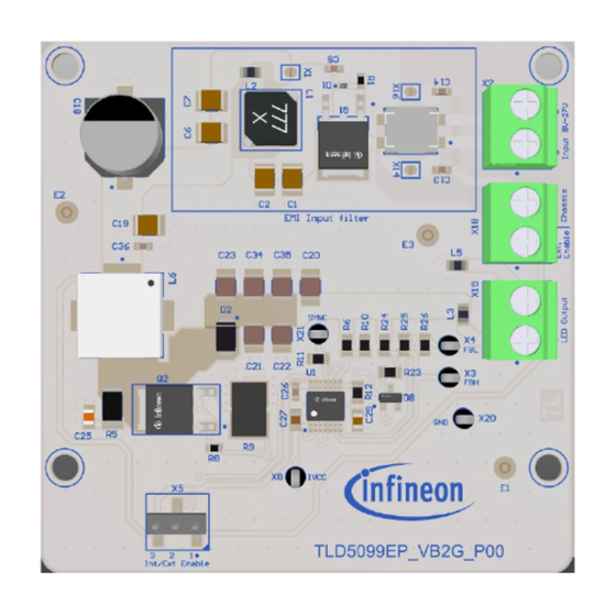
Page 2: Description
1 Description Description Evaluation board for high power LED application with TLD5099EP product in boost to ground topology. Default configuration of the board is boost to ground topology without any additional features enabled. In this configuration, it can deliver up to 13 W to the load with an efficiency above 90%. Auxiliary circuits, which protect the DC-DC and the load during short to ground, are present. - Page 3 Boost to ground evaluation kit TLD5099EP 1 Description Figure 2 Simplified schematic Table 1 Performance summary Parameter Conditions Value Input supply voltage Jumper X9 in position 2-3 (CCSC deactivated) 8 V to 27 V Parameter degradation below 6.5 V Down to 6.5 V for less than 2 s...
-
Page 4: Quick Start Procedure
Boost to ground evaluation kit TLD5099EP 2 Quick start procedure Quick start procedure The default configuration of the board has all additional features disabled. In this configuration the output current cannot be adjusted. The PWM signal has to be applied as digital signal on connector X18 (max. 45 V). -
Page 5: Current Adjustment
Boost to ground evaluation kit TLD5099EP 3 Current adjustment Current adjustment The output current adjustment can be performed by changing the value of trimmer R15 with a screwdriver, when jumper X10 is closed in position 1-2 and jumper X12 is closed. The output current can vary from 0 to 100% of the maximum output current (in this evaluation board from 0 to 350 mA). -
Page 6: Power Derating (Battery Dependent Current)
For example, if the power derating should start when the battery voltage drops under 12 V, R14 must be replaced with a 68 kΩ 0603 resistor (please refer to the TLD5099EP datasheets for more information). The PWM signal has to be applied as digital signal on connector X18 (max. 45 V). -
Page 7: Embedded Pwm Engine
100%. Closing jumper X6, the duty cycle is adjustable by means of trimmer R4. The PWM frequency is set to 350 Hz. If another PWM frequency is needed, C28 must be changed to a proper value (please refer to the TLD5099EP datasheets for more information). Jumpers are positioned as follows:... -
Page 8: Cold Crank Survival Circuit
This feature helps the system to survive LV124 test E11 “severe test pulse”, when the input voltage drops below 4.5 V, which is the minimum input voltage for the TLD5099EP. This circuit feeds back the device with the output voltage when the input voltage drops. To activate this feature, close jumper X9 in position 1-2. Other settings can be left as preferred. -
Page 9: Schematics
Boost to ground evaluation kit TLD5099EP 7 Schematics Schematics Figure 8 Input filter User Manual 2020-09-30... - Page 10 Boost to ground evaluation kit TLD5099EP 7 Schematics Figure 9 Main power User Manual 2020-09-30...
- Page 11 Boost to ground evaluation kit TLD5099EP 7 Schematics 7, 8 5, 6 Figure 10 Output stage User Manual 2020-09-30...
-
Page 12: Pcb Layout
Boost to ground evaluation kit TLD5099EP 8 PCB layout PCB layout Figure 11 PCB layout top view Figure 12 PCB layout bottom view User Manual 2020-09-30... -
Page 13: Bill Of Material
Boost to ground evaluation kit TLD5099EP 9 Bill of material Bill of material Table 6 Bill of material Designator Value Manufacturer Manufacturer order number C1, C2, C6, C7, C19, C31 10 uF Murata GCM32EC71H106KA03 C9, C26, C36 100 nF 06035C104K4Z2A... - Page 14 Boost to ground evaluation kit TLD5099EP 9 Bill of material Table 6 Bill of material (continued) Designator Value Manufacturer Manufacturer order number 2 kΩ Vishay CRCW08052K00FK 0 Ω Yageo AC0805JR-070RL R13, R20 22 kΩ Vishay CRCW060322K0FK 39 kΩ Vishay CRCW080539K0FK 560 Ω...
-
Page 15: Efficiency Measurements
Boost to ground evaluation kit TLD5099EP 10 Efficiency measurements Efficiency measurements Figure 13 Efficiency vs. input voltage This efficiency performance has been obtained with: Table 7 Parameters influencing efficiency Output load: Series of 12 white standard LED with Vj = 3 V kept cooled with forced air... -
Page 16: Maximizing Efficiency
Boost to ground evaluation kit TLD5099EP 11 Maximizing efficiency Maximizing efficiency This evaluation board has been designed to reach a fair compromise between efficiency performance and EM emissions compliance. Nevertheless, if the maximum efficiency is needed, the following actions should be considered:... -
Page 17: Minimizing Em Emissions
Boost to ground evaluation kit TLD5099EP 12 Minimizing EM emissions Minimizing EM emissions This evaluation board has been designed to reach a fair compromise between efficiency performance and EM conducted emissions compliance. Furthermore, this evaluation board can fulfill the class V of the CISPR25 in conducted emissions from 150 kHz to 108 MHz. -
Page 18: Revision History
Boost to ground evaluation kit TLD5099EP 13 Revision history Revision history Table 8 Revision history Document version Date of release Description of changes Rev. 1.00 2020-01-29 Initial release. Matching to evalboard S01_P01. Rev. 2.00 2020-09-30 Matching to evalboard S02_P02: •... -
Page 19: Disclaimer
Infineon Technologies, All Rights Reserved. information given herein in the real application. Infineon Technologies’ products may not be used in Infineon Technologies hereby disclaims any and all any applications where a failure of the product or warranties and liabilities of any kind (including without...
Need help?
Do you have a question about the TLD5099EP and is the answer not in the manual?
Questions and answers