Table of Contents
Advertisement
Quick Links
Z8F80411563
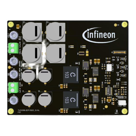
TLD6098-2DPVB2G_EVAL board
User guide
LITIX™ Power
Multitopology DC-DC controller
About this document
The TLD6098-2ES device used in this evaluation board, is an AEC qualified dual channel DC-DC controller,
especially designed to be used as voltage regulator such as power supply or current regulator such as an LED
driver. Its main features are:
Wide input voltage up to 58 V and output voltage range up to 70 V
•
EMC optimized device
•
Overvoltage, short to ground, overcurrent, open feedback and overtemperature diagnostic output
•
Configurable control as constant voltage or constant current
•
Scope and purpose
The scope of this user guide is to provide instructions on the use of TLD6098-2ES Power dual phase
boost‑to‑ground TLD6098-2DPVB2G_EVAL board.
Intended audience
This document is intended for engineers who perform measurements and check performances with
TLD6098‑2EP Power dual phase boost to ground TLD6098-2DPVB2G_EVAL board.
Evaluation Board
This TLD6098-2DPVB2G_EVAL board is to be used during the design-in process for evaluating and measuring
multiphase topology with TLD6098-2ES.
Note:
PCB and auxiliary circuits are NOT optimized for final customer design.
User guide
www.infineon.com
Please read the sections "Important notice" and "Warnings" at the end of this document
Revision 1.00
2022-12-22
Advertisement
Table of Contents

Related Manuals for Infineon LITIX TLD6098-2ES


Summary of Contents for Infineon LITIX TLD6098-2ES
-
Page 1: About This Document
This TLD6098-2DPVB2G_EVAL board is to be used during the design-in process for evaluating and measuring multiphase topology with TLD6098-2ES. Note: PCB and auxiliary circuits are NOT optimized for final customer design. User guide Please read the sections “Important notice” and “Warnings” at the end of this document Revision 1.00 www.infineon.com 2022-12-22... -
Page 2: Important Notice
Boards provided by Infineon Technologies. The design of the Evaluation Boards and Reference Boards has been tested by Infineon Technologies only as described in this document. The design is not qualified in terms of safety requirements, manufacturing and operation over the entire operating temperature range or lifetime. -
Page 3: Safety Precautions
TLD6098-2DPVB2G_EVAL User guide Safety precautions Safety precautions Note: Please note the following warnings regarding the hazards associated with development systems. Table 1 Safety precautions Warning: The evaluation or reference board contains DC bus capacitors which take time to discharge after removal of the main supply. Before working on the drive system, wait five minutes for capacitors to discharge to safe voltage levels. -
Page 4: Table Of Contents
TLD6098-2DPVB2G_EVAL User guide Table of contents Table of contents About this document ........................1 Important notice ..........................2 Safety precautions .......................... 3 Table of contents ..........................4 The board at a glance ......................5 Main features ............................6 Board parameters and technical data ....................6 System and functional description ................... -
Page 5: The Board At A Glance
TLD6098-2DPVB2G_EVAL User guide The board at a glance The board at a glance The TLD6098-2DPVB2G_EVAL dual phase boost-to-ground evaluation board is a switching power supply that, under nominal conditions, can deliver a constant voltage at the output between 43 V and 52 V and a current up to 7 A. -
Page 6: Main Features
TLD6098-2DPVB2G_EVAL User guide The board at a glance Figure 2 Simplified schematic Main features Ripple on input and output is reduced • Phase shift applied between the switching signal of channels • Frequency can be lowered which decreases the commutation losses •... -
Page 7: System And Functional Description
TLD6098-2DPVB2G_EVAL User guide System and functional description System and functional description The power supply is composed of two DC-DC channels that work in parallel. Channel 1 leads the output voltage, channel 2 follows channel 1. Channel 1 works as a constant voltage source, whereas channel 2 works as a current source. -
Page 8: Input Connection
TLD6098-2DPVB2G_EVAL User guide System and functional description Input connection The board is equipped with a double type connector both in the input and in the output: screw terminal blocks and 4 mm female bananas. Attention: The screw terminal blocks have a limited current capability of up to 20 A. If the input current is higher than 20 A or it is unknown, connect the input power supply by using female bananas connectors. - Page 9 TLD6098-2DPVB2G_EVAL User guide System and functional description As already mentioned in Chapter 2.1, above, when the output current of channel 1 causes a drop voltage on the shunt resistor R , higher than a certain threshold called V , a current loop takes over the DC-DC control I-SENSE REF1 and limits the output current in order to keep the drop voltage on the shunt to V...
-
Page 10: Output Voltage Regulation
TLD6098-2DPVB2G_EVAL User guide System and functional description Output voltage regulation Output voltage can be set between 43 V and 52 V. Figure 6 Output voltage regulation Overvoltage protection is set by voltage divider R = 68 kΩ and R = 1.8 kΩ. If during a fault the output VFBH-2 VFBL-2 voltage goes higher than 62 V, on pin VFB2 the voltage is higher 1.6 V and the switching activity is stopped until... - Page 11 TLD6098-2DPVB2G_EVAL User guide System and functional description Figure 8 FLT1 and FLT2 test points In this board FPWM/FAULT1,2 pins react as follows, to a fault: Table 4 Fault detection Fault type FPWM/FAULT1 (Yellow LED) FPWM/FAULT2 (Red LED) Constant voltage out enabled Continuous high N.A.
-
Page 12: Current Derating
TLD6098-2DPVB2G_EVAL User guide System and functional description Current derating Input current increases with the decreasing of input voltage. Thus, in order to keep components within their safety temperature, output power must be limited, reducing the output current according to the safe operating area (SOA) showed in the figure below. -
Page 13: System Design
TLD6098-2DPVB2G_EVAL User guide System design System design Schematics Figure 10 Top Level User guide Revision 1.00 2022-12-22... - Page 14 TLD6098-2DPVB2G_EVAL User guide System design Figure 11 Main power schematic User guide Revision 1.00 2022-12-22...
-
Page 15: Pcb Layout
TLD6098-2DPVB2G_EVAL User guide System design PCB layout Figure 12 Top overlay Figure 13 Internal overlay 1 (GND ground plane) User guide Revision 1.00 2022-12-22... - Page 16 TLD6098-2DPVB2G_EVAL User guide System design Figure 14 Internal overlay 2 Figure 15 Bottom overlay User guide Revision 1.00 2022-12-22...
-
Page 17: Bill Of Material
GCM21BR71C475KA73 D1, D2 STPS5L60SFY STMicroelectronics STPS5L60SFY 1SS389 Toshiba 1SS389 FLT1, FLT2, IVCC, SWN1, SWN2, VFB1, Keystone Electronics Corp. 5001 VFB2, VOUT, VSET1 Infineon Technologies TLD6098-2ES L1, L2 6.8 µH Coilcraft XAL1510-682MED Yellow Vishay TLMY1000-GS08 Vishay TLMS1100-GS08 Blue Wurth Elektronik 150060BS75000... - Page 18 TLD6098-2DPVB2G_EVAL User guide System design Designator Value Manufacturer Manufacturer order number R25, R29 0 Ω Vishay CRCW08050000Z0EAHP R26, R30 3 mΩ Bourns CRE2512-FZ-R003E-3 4.53 kΩ Vishay CRCW08054K53FK 30 mΩ Panasonic ERJC1CFR03U X1, X2 Phoenix Contact 1935776 X3, X4, X5, X6 Keystone Electronics Corp.
-
Page 19: Electrical Performance
TLD6098-2DPVB2G_EVAL User guide System design Electrical performance Figure 16 Input currents, switching nodes, output voltage (V = 12 V, V = 48 V, I = 7 A) Figure 17 Load dump (V = 14 V, V = 48 V, I = 0 A to 7 A, Rise time <... -
Page 20: Efficiency Measurements
TLD6098-2DPVB2G_EVAL User guide System design Efficiency measurements Efficiency vs. Input Voltage Input Voltage [V] Figure 18 Efficiency vs. input voltage performance This efficiency performance has been obtained with: Table 6 Efficiency measurement conditions Output load: Constant current sink set at 7 A Output voltage: 48 V Ambient temperature:... -
Page 21: Thermal Performances
TLD6098-2DPVB2G_EVAL User guide System design Thermal performances Ideally, the output current should be generated equally by both channels. Unfortunately, since the controller inputs FBH2 and FBL2 are real and show a residual offset, the currents sourced by the two channels are not identical. -
Page 22: References
TLD6098-2DPVB2G_EVAL User guide References References Infineon TLD6098-1EP Datasheet, https://www.infineon.com/cms/en/product/power/lighting-ics/litix- automotive-led-driver-ic/litix-power/tld6098-1ep/ Infineon TLD6098-2ES Datasheet, https://www.infineon.com/cms/en/product/power/lighting-ics/litix- automotive-led-driver-ic/litix-power/tld6098-2es User guide Revision 1.00 2022-12-22... -
Page 23: Revision History
TLD6098-2DPVB2G_EVAL User guide Revision history Revision history Document Date Description of changes revision Rev.1.00 2022-12-22 First release related to evalboard S03_P02 User guide Revision 1.00 2022-12-22... -
Page 24: Disclaimer
For information on the types in question please contact your nearest Published by Infineon Technologies office. Except as otherwise explicitly approved by Infineon Infineon Technologies AG Technologies in a written document signed by 81726 Munich, Germany authorized...
Need help?
Do you have a question about the LITIX TLD6098-2ES and is the answer not in the manual?
Questions and answers