Table of Contents
Advertisement
Quick Links
Z8F80286003
TLD5191HB2W-EVAL board
User guide
™
LITIX
Power TLD5191ES
About this document
Board description
™
•
LITIX
Power TLD5191ES: 4-switch buck-boost DC-DC controller designed for automotive applications
•
Constant output current (LED driver)
•
High power, high efficiency buck-boost architecture
•
Slow switches configuration to switch between different load conditions
•
EMC-optimized device: Spread spectrum (always ON)
Scope and purpose
The purpose of this user guide is to provide instructions for using the TLD5191ES device evaluation board
TLD5191HB2W-EVAL schematic version S01, PCB version P01.
The TLD5191HB2W-EVAL is an evaluation platform for the TLD5191ES, which can work as a buck-boost LED
driver, and features slow switches circuitry to change load conditions.
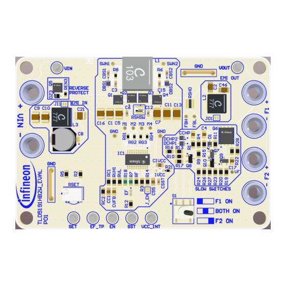
Figure 1
TLD5191HB2W-EVAL board
Intended audience
Hardware engineers
User guide
Please read the sections "Important notice" and "Warnings" at the end of this document
www.infineon.com
Rev. 1.00
2022-04-05
Advertisement
Table of Contents

Related Manuals for Infineon TLD5191HB2W-EVAL


Summary of Contents for Infineon TLD5191HB2W-EVAL
-
Page 1: About This Document
The purpose of this user guide is to provide instructions for using the TLD5191ES device evaluation board TLD5191HB2W-EVAL schematic version S01, PCB version P01. The TLD5191HB2W-EVAL is an evaluation platform for the TLD5191ES, which can work as a buck-boost LED driver, and features slow switches circuitry to change load conditions. -
Page 2: Table Of Contents
TLD5191HB2W-EVAL board User guide Table of contents Table of contents About this document ..............1 Table of contents . -
Page 3: Description
The TLD5191ES provides digital and analog dimming controls and one output flag for diagnostics. The TLD5191HB2W-EVAL is an evaluation platform for the TLD5191ES as LED driver. The default configuration delivers a constant current to LED load (1 A maximum). The output current can be... -
Page 4: Quick Start Procedure
TLD5191HB2W-EVAL board User guide 2 Quick start procedure Quick start procedure The Basic setup subchapter provides step-by-step instructions for setting up and running the TLD5191HB2W- EVAL. The board has two options for the enable signal: • J_EN closed: EN pin is connected to input supply line, so the device is immediately enabled when valid input voltage is applied •... - Page 5 TLD5191HB2W-EVAL board User guide 2 Quick start procedure Note: Output overvoltage protection is set to 23 V. Attention: To avoid a negative spike on the F2 MOSFET gate, in the case of high overvoltage threshold (> 25 V) and load on F2 composed of fewer than 2 LEDs, it is suggested to add a Schottky diode between its gate pin and GND.
-
Page 6: Electrical Characteristics
TLD5191HB2W-EVAL board User guide 3 Electrical characteristics Electrical characteristics Table 2 TLD5191HB2W-EVAL version S01 P01 electrical characteristics Parameter Symbol Values Unit Note or Test Condition Min. Typ. Max. Input voltage – Minimum value set by resistor divider on the EN/INUVLO pin Output voltage –... -
Page 7: Efficiency Measurements
TLD5191HB2W-EVAL board User guide 4 Efficiency measurements Efficiency measurements The following efficiency measurements have been taken with both functions active. For more information, refer Chapter 2.1. The efficiency discontinuities on the blue curve, result from changes in the controller mode from buck to buck-boost and from buck-boost to boost. -
Page 8: Additional Measurements
TLD5191HB2W-EVAL board User guide 5 Additional measurements Additional measurements Additional measurements to test the robustness of the design were conducted on this board. In particular, heavy LV124 stimuli were applied to the board input. Figure 5 LV124 E-06, Test Case #2... -
Page 9: Bill Of Material, Layout, And Schematic
TLD5191HB2W-EVAL board User guide 6 Bill of material, layout, and schematic Bill of material, layout, and schematic Table 4 Designator Value Footprint Quantity C1, C5, C9, C10, C16, C21 10 µF CAPC3225X270N-0 C2, C46 470 nF CAPC3216X178N C3, C15 470 pF... - Page 10 TLD5191HB2W-EVAL board User guide 6 Bill of material, layout, and schematic Table 4 (continued) BOM Designator Value Footprint Quantity 44.2 kΩ RESC2113X50N R4, R10, R11, R13, R16, 10 kΩ RESC2113X50N R17, R20, R24, R26, R27, 910 Ω RESC2113X50N 4.7 Ω...
- Page 11 TLD5191HB2W-EVAL board User guide 6 Bill of material, layout, and schematic SWN1 SWN2 VOUT EMI OUT REVERSE PROTECT EMI IN RSHSW CCHP DCHP2 DCHP1 IVCC RSET SLOW SWITCHES F1 ON BOTH ON F2 ON EF_TP VCC_INT Figure 8 PCB layout top view...
- Page 12 TLD5191HB2W-EVAL board User guide 6 Bill of material, layout, and schematic Figure 10 PCB layer 3 Figure 11 PCB layout bottom view User guide Rev. 1.00 2022-04-05...
- Page 13 TLD5191HB2W-EVAL board User guide 6 Bill of material, layout, and schematic Figure 12 Schematic view User guide Rev. 1.00 2022-04-05...
-
Page 14: Revision History
TLD5191HB2W-EVAL board User guide Revision history Revision history Document Date of Description of changes version release Rev. 1.00 2022-04-05 • Initial release User guide Rev. 1.00 2022-04-05... -
Page 15: Disclaimer
Infineon Technologies, All Rights Reserved. information given herein in the real application. Infineon Technologies’ products may not be used in Infineon Technologies hereby disclaims any and all any applications where a failure of the product or warranties and liabilities of any kind (including without...
Need help?
Do you have a question about the TLD5191HB2W-EVAL and is the answer not in the manual?
Questions and answers