Table of Contents
Advertisement
Quick Links
Advertisement
Table of Contents

Subscribe to Our Youtube Channel
Related Manuals for PerfecTron OXY5323A


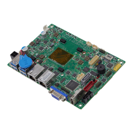
Summary of Contents for PerfecTron OXY5323A
- Page 2 Safety Information Electrical safety To prevent electrical shock hazard, disconnect the power cable from the electrical outlet before relocating the system. When adding or removing devices to or from the system, ensure that the power cables for the devices are unplugged before the signal cables are connected.
- Page 3 First release Packing List Item Description Q’ty OXY5323A Driver CD+ User’s manual Ordering information OXY5323A-01ET Intel®Apollo Lake-I E3930,DDR3L 1867 MHz, 1 x 204-pin SO-DIMM, Max. 8GB (Non-ECC),2 x Intel® I210-IT Giga LAN,4 x USB 3.0,1 x HDMI 1.4, 1 x VGA,2 x RJ-45,Normal Temperature: -20°C to 70°C OXY5323A-01UT Intel®Apollo Lake-I E3930,DDR3L 1867 MHz, 1 x 204-pin SO-DIMM, Max.
-
Page 4: Table Of Contents
Table of Contents Chapter 1 : Production Introduction ......................5 1.1 Block Diagram ............................5 1.2 Specifications ............................6 1.3 I/O Placement ............................7 Chapter 2 : Jumpers and Connectors ......................8 2.1 LVDS panel pin Header ........................8 2.2 eDP panel pin Header .......................... 9 2.3 Audio .............................. - Page 5 3.4 TRUSTED COMPUTING ........................35 3.5 SMART SETTINGS ..........................37 3.6 NCT6116D SUPER IO CONFIGURATION ..................38 3.7 S5 RTC WAKE SETTINGS(NO FUNCTION WHEN DEEPSX POWER POLICIES ENABLED) ..41 3.8 CPU CONFIGURATION ........................44 3.9 NETWORK STACK CONFIGURATION ..................... 50 3.10PLATFROM TRUST TECHNOLOGY....................
-
Page 6: Chapter 1 : Production Introduction
Chapter 1 : Production Introduction 1.1 Block Diagram... -
Page 7: Specifications
1.2 Specifications System Apollo Lake-M N3350/N4200 Apollo Lake-I E3930 Memory type DDR3L 1867 , 1 x 204-pin SO-DIMM, Max. 8GB (Non-ECC) Chipset Intel® SoC Integrated Graphics Intel® HD Graphics Ethernet 2 x Intel® I210-IT Giga LAN Audio> Realtek® ALC662 I/O Chipset Nuvoton NCT6116D Nuvoton NPCT650ABCYX TPM2.0 (Optional) Expansion... -
Page 8: I/O Placement
Power Requirement Power Input 8V to 24V Wide Range DC Input w/4-pin ATX connector (Pitch: 4.2mm) Environmental Operating Normal Temperature:-20°C to 70°C Temperature Wide Temperature (Optional*) : -40°C to 85°C Storage -40°C to 85°C (-40°F to 185°F) Temperature Operating 10% to 95% R/H, non-condensing Humidity Certification CE &... -
Page 9: Chapter 2 : Jumpers And Connectors
Chapter 2 : Jumpers and Connectors 2.1 FRONT_PANEL1 (JLVDS1) LVDS panel pin out define DEFINITION DEFINITION Minus signal of odd Minus signal of odd channel 0 (LVDS) channel 0 (LVDS) Plus signal of odd Plus signal of odd channel 0 (LVDS) channel 0 (LVDS) Minus signal of odd Minus signal of odd... -
Page 10: Edp Panel Pin Header
2.2 EDP1 Pin out define Signal Signal NC_ Reserved LCD_VCC High-speed _GND LCD_ Self _ Test-or- Lane3_N(DDPD_[3]N) LCD_GND Lane3_P(DDPD_[3]P) LCD_GND High-speed_ GND LCD_GND Lane2_N(DDPD_[2]N) LCD_GND Lane2_P(DDPD_[2]P) HDP(DDPD_HPD) High-speed_ GND BKLT_GND Lane1_N(DDPD_[1]N) BKLT_GND Lane1_P(DDPD_[1]P) BKLT_GND High-speed_ GND BKLT_GND Lane0_N(DDPD_[0]N) BKLT_ENABLE Lane0_P(DDPD_[0]P) BKLT_PWM_DIM High-speed_ GND NC_ Reserved... -
Page 11: Audio
BKLT_PS1 : Backlight inverter voltage selection header Pin Signal Description 5V option BKLT_PWR BKLT_PWR 12V option (default) FPD_PWR1 Pin out define Signal Description BKLT_EN Backlight enable BKLT_PWM Backlight control BKLT_PWR Backlight inverter power BKLT_PWR Backlight inverter power BKLT_GND/Brightness _GND Ground (shared) BKLT_GND/Brightness _GND Ground (shared) Brightness _Up Panel brightness increase... -
Page 12: 2Ea Lan Port
2.4 LAN port Diagram Color State Condition Link LAN link is not established Green LAN link is established Blinking LAN activity occurring Speed 10 Mb/s data rate Green 100 Mb/s data rate Yellow 1000 Mb/s data rate 2.5 SATA SATA PORT0: This is optional port from mini PCI-E and SATA0 Connector One fully-shrouded right angle internal SATA gen 3 ports (colored GREY) SATA PORT1 one fully-shrouded right ang... -
Page 13: Usb 2.0
2.8 USB Front panel USB header pin-out define (FP_USB1) Signal Signal FP_USB1 +5V DC +5V DC Data (negative) Data (negative) Data (positive) Data (positive) Ground Ground Key (no pin) No Connect Rear USB3.0 I/O port (J5/J10) Signal Name Description Mating Sequence J5/J10 Number VBUS... -
Page 14: Expansion Slot Layout
Follow the ATX specification and Industrial DFA (Design for Assembly) standard requirements for connector placement and spacing. Keep-out zone of PCI Express v3.0 x16 slot must allow use of double-width and long graphics cards without blocking access to any connectors (i.e. SATA ports, DIMM connector tabs, front panel audio header, …). 2.10 Expansion Slot Layout Slot Configuration Electrical... -
Page 15: Miapi Feature
2.12 J_MiAPI_1 Pin out define Signal Name Signal Name MAPI_GPIO1 MAPI_GPIO2 MAPI_GPIO6 MAPI_GPIO3 MAPI_GPIO7 MAPI_GPIO4 MAPI_GPIO8 MAPI_GPIO5 MAPI_GPIO9 Watchdog Timer MAPI_GPIO10 Power Button SMB_MAIN_DATA UART_TX SMB_MAIN_CLK UART_RX 5VSB 2.13 Serial Port J_RS485_P4, J_RS232_P2 Serial port header pin out define RXD# KEY (no pair) GROUND RTX TXD#... -
Page 16: At/Atx, Cmos , Msata Header In Silkscreen / Feature
2.14 AT/ATX, CMOS , mSATA header in silkscreen / feature (J_AT_CMOS1) pin out define JUMPER J_AT_CMOS1 (1-2) Clear CMOS (1-3) Normal (4-6) (6-8) (5-7) PCIE (5-7) NA mSATA JUMPER (1-2) (1-3) CMOS clear Normal: 1-3 Clear CMOS Clear CMOS Normal Clear CMOS: 1-2 JUMPER (8-6) -
Page 17: Atx Power 4P/Dc Power 4.2Mm Pin Header
2.16 ATX power 4P/DC power 4.2mm pin out define J_PW4P_1 signal Power 8V~24V Power 8V~24V... -
Page 18: Thermal Management And Fan Control
2.17 Thermal Management and Fan Control Nuvoton NCT6104D SuperIO: backup alternate solution as it leverages existing hardware in the designs, but software infrastructure must be put in place to support this solution. Regardless of solution chosen, BIOS/driver/tools support and subsystem validation is required, even if solution is not needed by pilot. -
Page 19: Fan Header Requirements
2.19 Fan Header Requirements The below requirements must be met for the 4- Closed loop fan speed control via the FANPWM0 signal routed to pin- Clearly label Locate closest to the CPU as required by the CDPG boxed CPU Chapter 3 : BIOS Specification This chapter provides information about how to set up BIOS and use BIOS menu items to adjust basic function settings. -
Page 23: Advanced Page
3.2 ADVANCED PAGE... -
Page 26: Intel(R) I210 Gigabit Network Connection - 00:22:4D:4D:00:01
3.2.1 INTEL(R) I210 GIGABIT NETWORK CONNECTION – 00:22:4D:4D:00:01... -
Page 28: Nic Configuration
3.2.2 NIC CONFIGURATION... -
Page 30: Intel(R) I210 Gigabit Network Connection - 00:22:4D:4D:00:02
3.2.3 INTEL(R) I210 GIGABIT NETWORK CONNECTION – 00:22:4D:4D:00:02... -
Page 31: Nic Configuration
3.2.4 NIC CONFIGURATION... -
Page 32: Driver Health
3.3DRIVER HEALTH... -
Page 34: Intel(R) Pro/1000 7.3.20 Pci-E
3.3.1 INTEL(R) PRO/1000 7.3.20 PCI-E... -
Page 36: Trusted Computing
3.4 TRUSTED COMPUTING... -
Page 38: Smart Settings
3.5 SMART SETTINGS... -
Page 39: Nct6116D Super Io Configuration
3.6 NCT6116D SUPER IO CONFIGURATION... -
Page 42: S5 Rtc Wake Settings(No Function When Deepsx Power Policies Enabled)
3.7 S5 RTC WAKE SETTINGS(NO FUNCTION WHEN DEEPSX POWER POLICIES ENABLED) -
Page 45: Cpu Configuration
3.8 CPU CONFIGURATION... -
Page 51: Network Stack Configuration
3.9 NETWORK STACK CONFIGURATION... -
Page 52: Platfrom Trust Technology
3.10PLATFROM TRUST TECHNOLOGY... -
Page 53: Chipset
3.11 CHIPSET... -
Page 59: Security
3.12 SECURITY... -
Page 61: Hdd Security Configuration
3.12.1 HDD SECURITY CONFIGURATION... -
Page 63: 2Secure Boot Mode
3.12.2SECURE BOOT MODE... -
Page 65: 3Key Managerment
3.12.3KEY MANAGERMENT... -
Page 70: Boot
3.13 BOOT... -
Page 74: Save & Exit
3.14 SAVE & EXIT...
Need help?
Do you have a question about the OXY5323A and is the answer not in the manual?
Questions and answers