Table of Contents
Advertisement
Quick Links
Advertisement
Table of Contents

Related Manuals for Advantech ROM-DB7502


Summary of Contents for Advantech ROM-DB7502
- Page 1 User Manual ROM-DB7502 Development Board for Qseven 2.0/2.1 modules...
- Page 2 No part of this manual may be reproduced, copied, translated or transmitted in any form or by any means without the prior written permission of Advantech Co., Ltd. Information provided in this manual is intended to be accurate and reliable. How- ever, Advantech Co., Ltd.
- Page 3 Consult the dealer or an experienced radio/TV technician for help. Ordering Information Part No. Description ROM-DB7502-SCA1E ROM-DB7502 Qseven 2.0/2.1 Carrier Board ROM-7510CD-PEA1E ROM-7510 Q7 TI AM5728DC 1.5GHz 0~60°C ROM-7510WD-PEA1E ROM-7510 Q7 TI AM5728 1.5GHz -40~85°C ROM-DK7510-F0A1E ROM-7510 Qseven 2.0 Development Kit Packing List Before installation, please ensure the following items have been shipped.
- Page 4 The equipment has been dropped and damaged. The equipment has obvious signs of breakage. DISCLAIMER: This set of instructions is given according to IEC 704-1. Advantech disclaims all responsibility for the accuracy of any statements contained herein. ROM-DB7502 User Manual...
- Page 5 Don't touch any components on the CPU card or other cards while the PC is on. Disconnect power before making any configuration changes. The sudden rush of power as you connect a jumper or install a card may damage sensitive elec- tronic components. ROM-DB7502 User Manual...
- Page 6 ROM-DB7502 User Manual...
-
Page 7: Table Of Contents
Introduction ....................2 Product Features..................2 Block Diagram................... 3 Reference document................. 3 1.4.1 Qseven standard SPEC..............3 1.4.2 ROM-DB7502 information............. 3 Chapter Installation........5 Module Form Factor.................. 6 Environmental Specifications ..............6 ROM-DB7501 Overview................7 Connector, Jumper setting, Switch and LED ..........8 2.4.1... - Page 8 ROM-DB7502 User Manual viii...
-
Page 9: Chapter 1 General Introduction
Chapter General Introduction This chapter gives background information on the ROM-DB7502. Sections include: Introduction Specification... -
Page 10: Introduction
It is compatible with ROM-7510 and has rich I/O interface for evaluation and development. It supports wide range operating temperatures, 2 power input inter- faces (one of them is designed for lithium-ion battery). ROM-DB7502 is an ideal development board for mobile applications, such as portable device, industrial tablet or HMI systems. -
Page 11: Block Diagram
SATA Pin box SATA Switch SPI Pin UART2 M.2 header Power/Sleep/Reset slot switch SDIO FAN SD slot conn Reference document 1.4.1 Qseven standard SPEC You can get the Qseven standard SPEC for SGET websit: https://www.sget.org/standards/qseven.html 1.4.2 ROM-DB7502 information ROM-DB7502 User Manual... - Page 12 ROM-DB7502 User Manual...
-
Page 13: Chapter 2 H/W Installation
Chapter H/W Installation This chapter gives mechanical and connector information on the ROM-DB7502 carrier board. Sections include: Connector Information Mechanical Drawing Hardware Installation... -
Page 14: Module Form Factor
The operating temperature refers to the environmental temperature for the model. Operating humidity: 5~95% relative humidity, non-condensing Storage temperature: -40~85° C Relative humidity: 95% @ 60° C Weight (g): 380 g (weight of total package) ROM-DB7502 User Manual... -
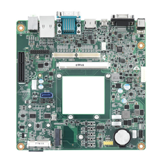
Page 15: Rom-Db7501 Overview
ROM-DB7501 Overview ROM-DB7502 User Manual... -
Page 16: Connector, Jumper Setting, Switch And Led
2.4.1.1 DCIN1 ROM-DB7502 Evaluation Board has a power connectors that can be used to power the board. The connector DCIN1 is a 12V +/-10% input. It must be used when the 12V voltage supply is required on the board (e.g. while using a cooling fan, a PCIe device or when this voltage is needed on the LVDS connector). - Page 17 GPIO2 General Purpose Input Output GPIO3 General Purpose Input Output GPIO4 General Purpose Input Output GPIO5 General Purpose Input Output GPIO6 General Purpose Input Output GPIO7 General Purpose Input Output GND_GPIO GND_IO Frame GND GND_IO Frame GND ROM-DB7502 User Manual...
- Page 18 2.4.1.3 USB OTG Connector (USB_OTG1) The ROM-DB7502 Evaluation Board has a standard Mini-USB interface for OTG Function. Pin Name DESCRIPTION +USB_OTG_5V_X Power USB_OTG-_X USB OTG differential signal USB_OTG+_X USB OTG differential signal USB_OTG_ID_X USB OTG ID ROM-DB7502 User Manual...
- Page 19 HDMI DATA2- HDMI_X_D1+ HDMI DATA1- HDMI_X_D1- HDMI DATA1+ HDMI_X_D0+ HDMI DATA0+ HDMI_X_D0- HDMI DATA0- HDMI_X_CK+ HDMI Clock+ HDMI_X_CK- HDMI Clock- HDMI_X_CEC HDMI CEC Signal HDMI_X_CTRL_CK HDMI DDC signal HDMI_X_CTRL_DAT HDMI DDC Signal +V5_HDMI_2 HDMI Power HDMI_X_HPD HDMI HotPlug ROM-DB7502 User Manual...
- Page 20 2.4.1.5 CAN BUS (CN8A) The ROM-DB7502 Evaluation Board uses the TI_SN65HVD251DR CAN transceiver to implement the CAN interface in conjunction with the A port on the ROM-DB7502 module. Pin Name DESCRIPTION CAN0_CONN_D- CAN BUS Data+ GND_SHIELD CAN0_CONN_D+ CAN BUS Data+...
- Page 21 2.4.1.6 RS232 (CN8B) The ROM-DB7502 Evaluation Board provides 4-wire UART to the connector CN8B (TOP) through an RS232 transceiver. Pin Name DESCRIPTION COM2_RX Serial Data Receiver COM2_TX Serial Data Transmitter GND_COM2 COM2_RTS Handshake signal, request to send data COM2_CTS Handshake signal, clear to send data...
- Page 22 2.4.1.7 RJ45 (CN2A) The ROM-DB7502 Evaluation Board provides an RJ45 connector with integrated magnetics for 10/100/1000Mb Ethernet. Pin Name DESCRIPTION GBE_LINK_ACT# Ethernet controller activity indicator active low. Ethernet controller 1000Mbit/sec link indicator active GBE_LINK1000# low. Ethernet controller 100Mbit/sec link indicator active...
- Page 23 USB OTG differential signal USB_HOST_DP_X USB OTG differential signal Signal GND USB1_SS_X_RX- USB3.0 differential RX signal USB1_SS_X_RX+ USB3.0 differential RX signal Signal GND USB1_SS_X_TX- USB3.0 differential TX signal USB1_SS_X_TX+ USB3.0 differential TX signal GND_GBE Frame Ground GND_GBE Frame Ground ROM-DB7502 User Manual...
- Page 24 USB 2.0 differential signal USB2_DP_X USB 2.0 differential signal Signal GND USB2_SS_X_RX- USB3.0 differential RX signal USB2_SS_X_RX+ USB3.0 differential RX signal Signal GND USB2_SS_X_TX- USB3.0 differential TX signal USB2_SS_X_TX+ USB3.0 differential TX signal GND_GBE Frame Ground GND_GBE Frame Ground ROM-DB7502 User Manual...
- Page 25 2.4.1.10 Audio Jack (AUDIO1) ROM-DB7502 evaluation board provides an audio interface, including MIC IN and head phone, using Codec module ROM-EG52, through the connector I2S_CN1 con- nected to the evaluation board, CODEC IC model for the TI_TLV320AIC3106IRGZT. Pin Name DESCRIPTION...
-
Page 26: Internal I/O
LVDS_VDD4 LVDS_BL2 LVDS1 Backlight Power Select USB_SW USB HOST & OTG switch SATADOM_PWR1 SATADOM & Normal SATA Switch SDIO_SW M.2 & SD card Function Switch CN11 Watchdog Time OUT# Jumper Thermal Down Jumper CN10 Boot Disable Jumper ROM-DB7502 User Manual... - Page 27 LVDS1 Backlight Power Select setting Function Pin1-Pin2 Chose 5V For LVDS1 Backlight Power Pin2-Pin3 Chose 12V For LVDS1 Backlight Power USB_SW USB HOST & OTG switch setting Function Pin1-Pin2 Chose USB signal to HOST Pin2-Pin3 Chose USB signal to OTG ROM-DB7502 User Manual...
- Page 28 Chose SDIO signal to M.2 CN11 Watchdog Time OUT# Jumper setting Function Pin1-Pin2 Connect to GND Pin2-Pin3 Thermal Down Jumper setting Function Pin1-Pin2 Connect to GND Pin2-Pin3 CN10 Boot Disable Jumper setting Function Pin1-Pin2 Connect to GND Pin2-Pin3 ROM-DB7502 User Manual...
- Page 29 Sleep Button Pin Header CN18 Power Button Pin Header SMART_FAN1 Smart Fan Connector CN13 EC Image Program Pin Header Li Batter Socket 2.4.2.1 BAT1 Pin Name DESCRIPTION BAT_THER BAT_ID_CN I2C_EC_DAT_3V3 I2C SDA I2C_EC_CK_3V3 I2C SCL +VBATT Power +VBATT Power ROM-DB7502 User Manual...
- Page 30 2.4.2.2 LCD Panel Connector (LVDS1) The ROM-DB7502 Evaluation Board provides many options for connecting LCD pan- els and monitors, with the following three interfaces supported: Dual Channel 24 bit LVDS Single Channel 24 bit LVDS HDMI Almost any TFT or STN display can be connected to the LVDS port of the ROM- DB7502 module by simply connecting the necessary signals from connectors LVDS1 and LVDS2 to the display.
- Page 31 LVDS0_CTRL LVDS0_CTRL 2.4.2.3 LVDS_BK_PWR1 Pin Name DESCRIPTION +VDD_BKLT_LVDS0 LVDS0 Backlight Power LCD1_BKLT_EN LVDS0 Backlight Enable Signal LCD1_BKLT_PWM LVDS0 Backlight Control signal Power ROM-DB7502 User Manual...
- Page 32 LVDS DATA0 LVDS1_X_D0+ LVDS DATA0 LVDS1_X_D1- LVDS DATA1 LVDS1_X_D1+ LVDS DATA1 LVDS1_X_D2- LVDS DATA2 LVDS1_X_D2+ LVDS DATA2 LVDS1_X_CK- LVDS Clock LVDS1_X_CK+ LVDS Clock LVDS1_DID_CK LVDS EDID LVDS1_DID_DAT LVDS EDID LVDS1_X_D3- LVDS DATA3 LVDS1_X_D3+ LVDS DATA3 LVDS1_CTRL LVDS0_CTRL ROM-DB7502 User Manual...
- Page 33 2.4.2.5 LVDS_BK_PWR2 Pin Name DESCRIPTION +VDD_BKLT_LVDS1 LVDS1 Backlight Power LCD2_BKLT_EN LVDS1 Backlight Enable Signal LCD2_BKLT_PWM LVDS1 Backlight Control signal Power ROM-DB7502 User Manual...
- Page 34 2.4.2.6 PCIE slot (CN16) The ROM-DB7502 Evaluation Board has a standard 4 Lane PCI Express interface. Pin Name DESCRIPTION +V12 Power +V12 Power +V12 Power Power PCIEX_A_JTAG1 +V3A Power Sideband wake signal asserted by components requesting PCIE_A_WAKE# wakeup. PCIE_A_X_TX+ PCI Express channel 0, Transmit Output differential pair...
- Page 35 PCI Express channel 1, Receive Input differential pair PCIE_C_X_RX+ PCI Express channel 2, Receive Input differential pair PCIE_C_X_RX- PCI Express channel 2, Receive Input differential pair PCIE_D_X_RX+ PCI Express channel 3, Receive Input differential pair PCIE_D_X_RX- PCI Express channel 3, Receive Input differential pair ROM-DB7502 User Manual...
- Page 36 User Identity Module Reset W_DISABLE# Disable Module Card PERST# force a hardware reset on the card I2C SCL signal I2C SDA signal USB1- USB signal USB1+ USB signal +3.3V_PCIe Power +3.3V_PCIe Power LED_WWAN# status indicators LED_WLAN# status indicators ROM-DB7502 User Manual...
- Page 37 LED_WPAN# status indicators ROM-DB7502 User Manual...
- Page 38 2.4.2.8 SIM Card Socket (CN15) Pin Name DESCRIPTION UIM_VCC Power UIM_RESET1 UIM reset signal UIM_CLK_R UIM clock signal UIM_DATA UIM data signal. ROM-DB7502 User Manual...
- Page 39 2.4.2.9 SD Card Socket (SD1) The ROM-DB7502 Evaluation Board features 4-bit SDIO interfaces. Pin Name DESCRIPTION SDIO Data.These signals operate in push- SDIO_DATA3_X pull mode SDIO Command/Response. This signal is used for card initialization and for com- SDIO_CMD_X mand transfers. During initialization mode this signal is open drain.
- Page 40 12V Power 2.4.2.11 SATA Signal Connector (SATA1) The ROM-DB7502 Evaluation board supports the Serial ATA (SATA) interface on the ROM-DB7502 module and allows peripherals such as external hard drives, SSDs and SATA DOM to be connected. Jumper SATADOM_PWR1 determines whether the connected peripherals are SATA- DOM or standard SATA.
- Page 41 2.4.2.12 Debug Port (JTAG) The ROM-DB7502 Evaluation Board provides a JTAG interface to the JTAG port available on ROM-7510 modules. Connector JTAG provides an interface to an external JTAG device via a standard 2.00mm pin header connector. Pin Name DESCRIPTION...
- Page 42 UART Clear To Send UART4_RTS_1V8 UART Ready To Send NFC_WI_IN Vendor Defined Suspend Clock is a 32.768 kHz clock supply input SUS_CLK that is provided by platform to enable the add-in card to enter reduce power consumption modes ROM-DB7502 User Manual...
- Page 43 W_DISABLE2# disable radio operation W_DISABLE1# disable radio operation +3.3V_M2 Power +3.3V_M2 Power ROM-DB7502 User Manual...
- Page 44 ROM-DB7502 User Manual...
- Page 45 Master clock input AUDIO_I2C_CK I2C SCL MIC_BIAS Microphone bias voltage output AUDIO_I2C_DAT I2C SDA GND_AUD Frame GND HP_R High-power output driver (right +) MIC_IN MIC3 input GND_AUD Frame GND GND_AUD Frame GND HP_L High-power output driver (left +) ROM-DB7502 User Manual...
- Page 46 Master serial output/Slave serial input signal. SPI SPI0_MOSI serial output data from Qseven® module to the SPI device Master serial input/Slave serial output signal. SPI SPI0_MISO serial input data from the SPI device to Qseven® mod- ule. SPI0_CS1# SPI Chip Select 1 signal ROM-DB7502 User Manual...
- Page 47 2.4.2.17 5V Power LED Pin Header (PWRLED1) Pin Name DESCRIPTION Power 2.4.2.18 GPII0 Pin Header (CN4) Pin Name DESCRIPTION GPII0 GPII Signal 2.4.2.19 Reset Button Pin Header (CN19) Pin Name DESCRIPTION RESET_IN# Reset Signal ROM-DB7502 User Manual...
- Page 48 2.4.2.22 Smart Fan Connector (SMART_FAN1) The ROM-DB7502 Evaluation board provides a FAN connector, SMART_FAN1. The 12V or 5V supply which is available at this connector is connected to the 12V or 5V regulated power supply using a Jumper which is controlled by CN6.
- Page 49 A 20 mm (diameter) coin cell/battery should be used with the Battery Holder (BH1). A coin cell battery can be used to provide power backup to the external RTC circuits when external power supply is not available. Supported batteries: CR2032 or similar coin cells. Pin Name DESCRIPTION +BAT_RTC Power ROM-DB7502 User Manual...
-
Page 50: Hardware Installation
Install the ROM-7510 module board to carrier board at a 30 degree angle. Press down the module board and make sure the 4 screw holes are aligned with the carrier board and adjust the 4 screws clockwise to fix them in place ROM-DB7502 User Manual... -
Page 51: Chapter 3 Advantech Service
Chapter Advantech Service Advantech design in service, technical support and warranty policy for evaluation kit. -
Page 52: Risc Design-In Services
Easy Development Advantech has support firmware, root file-system, BSP or other develop tools for cus- tomers. It helps customers to easy develop their carrier board and differentiate their embedded products and applications. - Page 53 Advantech has been involved in the industrial computer industry for many years and found that customers usually have the following questions when implementing modu- lar designs.
- Page 54 RISC COM. Design stage When a product moves into the design stage, Advantech will supply a design guide of the carrier board for reference. The carrier board design guide provides pin defini- tions of the COM connector with limitations and recommendations for carrier board design, so customers can have a clear guideline to follow during their carrier board development.
-
Page 55: Contact Information
RISC platforms usually have less support for ready-made drivers on the carrier board, therefore the customer has to learn from trial and error and finally get the best solution with the least effort. Advantech’s team has years of experience in customer support and HW/SW development knowledge. Conse- quently, we can support customers with professional advice and information as well as shortening development time and enabling more effective product integration. -
Page 56: Global Service Policy
(Dead-on-Arrival). The DOA Cross-Shipment excludes any shipping damage, cus- tomized and/or build-to-order products. For those products which are not DOA, the return fee to an authorized ADVANTECH repair facility will be at the customers' expense. The shipping fee for reconstructive products from ADVANTECH back to customers' sites will be at ADVANTECH's expense. -
Page 57: Repair Process
"Problem D escription". Vague entries such as "does not work" and "failure" are not acceptable. If you are uncertain about the cause of the problem, please contact ADVANTECH's Application Engineers (AE). They may be able to find a solution that does not require sending the product for repair. - Page 58 Product updates and tests upon the request of customers who are without war- ranty. If a product has been repaired by ADVANTECH, and within three months after such a repair the product requires another repair for the same problem, ADVANTECH will do this repair free of charge.
- Page 59 3.3.2.6 Shipping Back to Customer The forwarding company for RMA returns from ADVANTECH to customers is selected by ADVANTECH. Per customer requirement, other express services can be adopted, such as UPS, FedEx and etc. The customer must bear the extra costs of such alternative shipment.
- Page 60 No part of this publication may be reproduced in any form or by any means, electronic, photocopying, recording or otherwise, without prior written permis- sion of the publisher. All brand and product names are trademarks or registered trademarks of their respective companies. © Advantech Co., Ltd. 2017...
Need help?
Do you have a question about the ROM-DB7502 and is the answer not in the manual?
Questions and answers