Table of Contents
Advertisement
Quick Links
Advertisement
Table of Contents

Related Manuals for Advantech ROM-DB3900


Summary of Contents for Advantech ROM-DB3900
- Page 1 User Manual ROM-DB3900 Development Board for RTX v2.0 Modules...
- Page 2 No part of this manual may be reproduced, copied, translated or transmitted in any form or by any means without the prior written permission of Advantech Co., Ltd. Information provided in this manual is intended to be accurate and reliable. How- ever, Advantech Co., Ltd.
- Page 3 Increase the separation between the equipment and receiver. Connect the equipment into an outlet on a circuit different from that to which the receiver is connected. Consult the dealer or an experienced radio/TV technician for help. ROM-DB3900 User Manual...
- Page 4 USB 4 pin to Type A Cable 1700022373-01 Debug port cable for ROM-3420 1700019474 A Cable D-SUB 9P(F)/D-SUB 9P(F) RS232/RS485 100c 2026390000 China RoHS ROM-DB3900 Electronic Pollution 1st Optional Accessories Part No. Description 9696MEG510E Daughter board for audio codec 9696MX5300E...
- Page 5 ROM-3420CQ-MDA1E Freescale i.mx6 Quad core 1GHz with 1GB memory(0~60C) ROM-3420WQ-MDA1E Freescale i.mx6 Quad core 1GHz with 1GB memory(-40~85C) For more information please refer to "Advantech Baseboard Check List" and "Evalu- ation Board Reference Schematic". You can download "Advantech Baseboard Check List" and "Evaluation Board Refer- ence Schematic"...
- Page 6 The sound pressure level at the operator's position according to IEC 704-1:1982 is no more than 70 dB (A). DISCLAIMER: This set of instructions is given according to IEC 704-1. Advantech disclaims all responsibility for the accuracy of any statements contained herein.
- Page 7 ......1 Introduction ....................2 Product Specification ................2 Chapter Installation........3 Module Form Factor.................. 4 Environmental Specifications ..............4 ROM-DB3900 Appearance ............... 4 2.3.1 ROM-DB3900 Overview ............... 4 2.3.2 I/O Connectors................5 Connectors, Jumper settings, Switches and LEDs ........5 2.4.1 Rear I/O panel................
-
Page 8: Table Of Contents
Obtaining an RMA Number............39 3.5.2 Returning the Product for Repair ..........39 3.5.3 Service Charges ................. 40 3.5.4 Repair Report ................41 3.5.5 Custody of Products Submitted for Repair ......... 41 3.5.6 Shipping Back to Customer ............41 ROM-DB3900 User Manual viii... - Page 9 Chapter General Introduction This chapter gives background information on the ROM-DB3900. Sections include: Introduction Specification...
- Page 10 Introduction ROM-DB3900 is an evaluation carrier board designed for the Advantech RTX mod- ule. It is compatible with RTX module ROM-3420 and has rich I/O interface for evalu- ation and development. It supports wide range operating temperatures, and also supports two MIPI connectors for the camera module. ROM-DB3900 is an ideal development board for ruggedized applications, such as medical device, Industrial control, Transportation/fleet management systems.
- Page 11 Chapter H/W Installation This chapter gives mechanical and connector information on the ROM-DB3900 carrier board. Sections include: Connector Information Mechanical Drawing Hardware Installation...
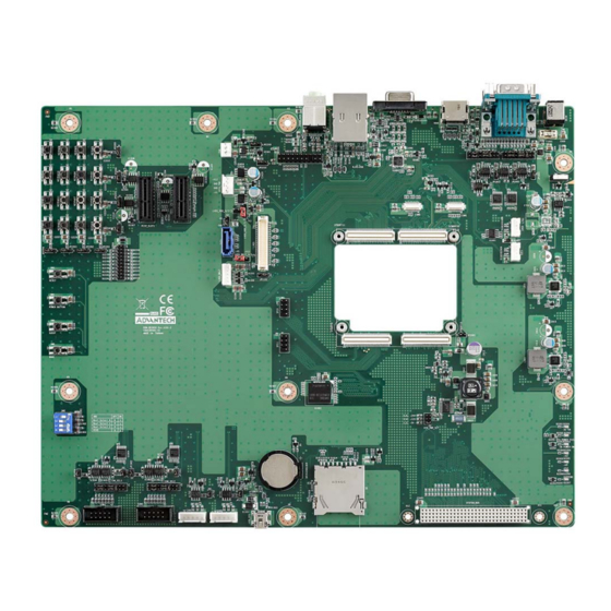
- Page 12 The operating temperature refers to the environmental temperature for the model. Operating humidity: 0% ~ 90% relative humidity, non-condensing Storage temperature: -40~85 °C Relative humidity: 95% @ 60 °C Weight (g): 80 g (weight of total package) ROM-DB3900 Appearance 2.3.1 ROM-DB3900 Overview ROM-DB3900 User Manual...
- Page 13 UART Port 1 COM01B UART Port 2 HDMI HDMI Port VGA Port RJ45+USB GbE Ethernet Connector RJ45+USB USB Port 1/ 2 PHONE_JACK MIC Input/ Audio Output Table 2.2: DCIN (DC-Jack, +19V power input) Signal Signal +19V Shield ROM-DB3900 User Manual...
- Page 14 Table 2.3: COM01A (UART0, 4 WIRE) Signal Signal TXD485- RXD/TXD485+ TXD/RXD485+TX RXD485- Table 2.4: COM01B (UART1, 4 WIRE) Signal Signal TXD485- RXD/TXD485+ TXD/RXD485+ RXD485- ROM-DB3900 User Manual...
- Page 15 Table 2.5: VGA (VGA) Signal Signal Green Blue DDC_DAT HSYNC VSYNC DDC_CK Table 2.6: HDMI (HDMI) Signal Signal TMDS_D2+ TMDS_D2- TMDS_D1+ TMDS_D1- TMDS_D0+ TMDS_D0- TMDS_CLK+ TMDS_CLK- CTRL_CLK CTRL_DAT ROM-DB3900 User Manual...
- Page 16 Table 2.7: RJ45+USB (RJ-45 & USB 1/2) Signal VBUS SS_RX- SS_RX+ GBE_LINK1000# SS_TX- SS_TX+ Table 2.8: PHONE_JACK (Audio output) Signal Signal Audio_L Audio_R MIC_IN Line out: stereo, Line in: mono ROM-DB3900 User Manual...
- Page 17 Serial ATA 7P 1.27mm 180D(M) DIP WATM- SATA SATA 07DBN4A3B8 GPIO GPIO PIN HEADER 10x2P 2.0mm 180D(M) DIP 21N22050 WAFER BOX 2.0mm 5P 180D(M) DIP WO/Pb JIH LVDS_BKLT LVDS Backlight Reset button TACT SW STS-091 SMD 4P H=3.8mm ROM-DB3900 User Manual...
- Page 18 PCB SKT 30x4P 2.00mm 180D(F) DIP 264-40303-02 WAFER BOX 2.0mm 4P 180D(M) W/LOCK I2C0 I2C0 A2001WV2-4P WAFER BOX 2.0mm 4P 180D(M) W/LOCK I2C1 I2C1 A2001WV2-4P RTXA,RTXB, RTX B2B B/B Conn. 50x2P 0.5mm 180D(M) SMD RTXC,RTXD Connector AXK500137YG ROM-DB3900 User Manual...
- Page 19 2.4.3 Connectors Table 2.10: PCIE_SLOT0 (PCIex1 connector1) Signal Signal +12V +12V +12V +12V +12V +12V PCIE_A_CK PCIE_A_JTAG2 PCIE_A_DAT PCIE_A_JTAG3 PCIE_A_JTAG4 PCIE_A_JTAG5 PCIE_A_JTAG1 PWRGD Mechanical Key Reserved PCIE_A_REFCK+ PCIE_A_TX+ PCIE_A_REFCK- PCIE_A_TX- PCIE_A_RX+ PCIE_A_RX- ROM-DB3900 User Manual...
- Page 20 Table 2.11: PCIE_SLOT1 (PCIex1 connector2) Signal Signal +12V +12V +12V +12V +12V +12V PCIE_B_CK PCIE_B_JTAG2 PCIE_B_DAT PCIE_B_JTAG3 PCIE_B_JTAG4 PCIE_B_JTAG5 PCIE_B_JTAG1 PWRGD Mechanical Key Reserved PCIE_B_REFCK+ PCIE_B_TX+ PCIE_B_REFCK- PCIE_B_TX- PCIE_B_RX+ PCIE_B_RX- ROM-DB3900 User Manual...
- Page 21 Table 2.12: SATA (SATA connector) Signal Signal SATA_TX+ SATA_TX- SATA_RX- SATA_RX+ SATA DOM PIN7 Table 2.13: SATA_PWR (SATA Power connector) +12V ROM-DB3900 User Manual...
- Page 22 LVDS_D2- LVDS_D2+ LVDS_CLK- LVDS_CLK+ DID_CK DID_DAT EDP_HDP LVDS D3- LVDS D3+ LVDS_CTRL Table 2.15: LVDS_BKLT (LVDS backlight power) Signal Signal +VDD_BKLT_LVDS BLK_EN Brightness Table 2.16: USB_OTG (USB OTG) Signal Signal VBUS USB_OTG D- USB_OTG D+ OTG ID ROM-DB3900 User Manual...
- Page 23 SDIO_DATA3_X SDIO_CMD SDIO_CK SDIO_DATA0 SDIO_DATA1 SDIO_DATA2 SDIO_CD# +3V_SDIO Table 2.18: BR2032HOLDER (CR-2032) Signal Signal BAT_RTC 2.4.4 Jumpers Table 2.19: JP2201 (GPIO/Keypad selection for GPIO0/10) Signal GPIO0 GPIO10 Table 2.20: JP2202 (GPIO/Keypad selection for GPIO1/11) Signal GPIO1 GPIO11 ROM-DB3900 User Manual...
- Page 24 Table 2.22: JP2204 (GPIO/Keypad selection for GPIO3/13) Signal GPIO3 GPIO13 Table 2.23: JP2205 (GPIO/Keypad selection for GPIO4/14) Signal GPIO4 GPIO14 Table 2.24: JP2206 (GPIO/Keypad selection for GPIO5/15) Signal GPIO5 GPIO15 Table 2.25: JP2207 (GPIO/Keypad selection for GPIO6/16) Signal GPIO6 GPIO16 ROM-DB3900 User Manual...
- Page 25 Table 2.26: JP2208 (GPIO/Keypad selection for GPIO7/17) Signal GPIO7 GPIO17 Table 2.27: JP2208 (GPIO8) Signal GPIO8 Table 2.28: JP22 (GPIO9) Signal GPIO9 Table 2.29: JP1801~JP1804, JP1901~JP1904 (UART 120om terminal resister) Signal 120 OM (Default) Without 120 OM ROM-DB3900 User Manual...
- Page 26 Mode Jumper Mode 120 OM (Default) Without 120 OM Table 2.33: JP1702 (CAN1 bus, 120OM terminal resistor) Jumper Mode Jumper Mode 120 OM (Default) Without 120 OM Jumper Mode Jumper Mode 120 OM (Default) Without 120 OM ROM-DB3900 User Manual...
- Page 27 Table 2.34: COM_SEL0/1/2/3 (UART0/1/2/3 function selection Signal Signal SER2_RX RXD485_A SER2_RX RXD422_A SER2_RX RXD232_A COM2_RXD NDCD#TXD485- NRXD2TXD485+ TXD485-_A TXD485+_A COM2_TXD NTXD2_RXD485+ NDTR#2_RXD485- RSD485+_A RSD485-_A Table 2.35: (UART1, 2wires) Signal Signal TXD485- COM1_RX COM1_TX RXD485- ROM-DB3900 User Manual...
- Page 28 Table 2.36: (UART3, 2wires) Signal Signal TXD485- RXD/TXD485+ TXD/RXD485+ RXD485- Table 2.37: CAM0 (Camera 1, MIPI) Signal Signal PCAM_HSYNC PCAM_ON_CSI1 PCAM_VSYNC PCAM_PXL_CK1 CAM0_PWR CAM0_RST I2C_CSI0_DAT I2C_CSI0_CK CSI0_X_CK+ CSI0_X_CK- PCAM_MCK CSI0_X_D1+ CSI0_X_D1- CSI0_MCK CSI0_D0+ CSI0_X_D0- ROM-DB3900 User Manual...
- Page 29 Signal Signal 3.3V GPIO8 GPIO9 GPIO0 KEY_SEL_ROW0 GPIO10 KEY_SEL_ROW0 GPIO1 KEY_SEL_ROW1 GPIO11 KEY_SEL_ROW1 GPIO2 KEY_SEL_ROW2 GPIO12 KEY_SEL_ROW2 GPIO3 KEY_SEL_ROW3 GPIO13 KEY_SEL_ROW3 GPIO4 KEY_SEL_COL0 GPIO14 KEY_SEL_COL0 GPIO5 KEY_SEL_COL1 GPIO15 KEY_SEL_COL1 GPIO6 KEY_SEL_COL2 GPIO16 KEY_SEL_COL2 GPIO7 KEY_SEL_COL3 GPIO17 KEY_SEL_COL3 ROM-DB3900 User Manual...
- Page 30 Table 2.40: JP2301 (External WDT) Signal Signal WDT_Time_Out# Table 2.41: FAN (System FAN) Signal Signal +12V Table 2.42: AUDIO (I2S0, audio codec) Signal Signal Audio_VDDA Audio_VDDA I2S0_SDIN_C I2S0_SDOUT_C I2S0_LRCK_C I2S0_CK_C AUDIO_MCK_C Audio_I2C_CK MIC_BIAS Audio_I2C_DAT HP_R MIC_IN HP_L ROM-DB3900 User Manual...
- Page 31 Table 2.44: SPI0 (SPI0) Signal Signal SPI0_CS0# SPI0_CK SPI0_DO_C SPI0_DIN_C SPI0_CS1#_C Table 2.45: LVDS_BK_SLT (LVDS backlight selection) Jumper Mode Jumper Mode +5V (Default) +12V * +VDD_BKLT_LVDS, pin1 Table 2.46: LVDS_VDD_SLT1 (LVDS VDD Power selection) Jumper Mode Jumper Mode +3.3V ROM-DB3900 User Manual...
- Page 32 Table 2.47: LVDS_VDD_SLT2 (LVDS VDD Power selection2) Jumper Mode Jumper Mode +12V Table 2.48: CAN0 (CAN bus 0) Signal Signal CAN0_D- CAN0_D+ Table 2.49: CAN0 (CAN bus 0) Signal Signal CAN0_D- CAN0_D+ ROM-DB3900 User Manual...
- Page 33 SYSBUS_A20 SYSBUS_A28 SYSBUS_A21 SYSBUS_A29 SYSBUS_A22 SYSBUS_A30 SYSBUS_A23 SYSBUS_INT0 SYSBUS_INT2 SYSBUS_INT1 SYSBUS_INT3 SYSBUS_ALE SYSBUS_WAIT# SYSBUS_BE0# SYSBUS_CS0# SYSBUS_BE1# SYSBUS_CS1# SYSBUS_WE# SYSBUS_OE# SYSBUS_CLK RESET_IN# I/PU RESET_OUT# WAKE# I/PU CB_PWR_EN SLEEP# I/PU CB_PGOOD I/PU SUSPEND_REQ# RTX_PGOOD I/PU WDT_OUT# RTC_PWR POWER_BTN# I/PU ROM-DB3900 User Manual...
- Page 34 SD0_WP I/PU TTL_G6 TTL_G7 SD0_CMD SD0_D0 TTL_B0 SD0_D1 TTL_B1 SD0_D2 TTL_B2 SD0_D3 TTL_B3 SD0_CLK TTL_B4 TTL_B5 VDD_SD1_EN TTL_B6 SD1_CD# I/PU TTL_B7 SD1_WP I/PU SD1_CMD SPI0_MISO SD1_D0 SPI0_MOSI SD1_D1 SPI0_CS0# SD1_D2 SPI0_CS1# SD1_D3 SPI0_CLK SD1_D4 SD1_D5 SPI1_MISO SD1_D6 ROM-DB3900 User Manual...
- Page 35 CSI1_D0- / PCAM_D3 DP/I PCAM_MCK CSI1_D0+ / PCAM_D2 DP/I PCAM_HSYNC CSI1_CK- / PCAM_D1 DP/I PCAM_VSYNC CSI1_CK+ / PCAM_D0 DP/I PCAM_DE PCAM_FLD CAM_MCK PCAM_PXL_CK1 PCAM_PXL_CK0 PCIE1_TX+ PCIE1_TX- PCIE0_TX+ PCIE0_TX- PCIE1_RX+ PCIE1_RX- PCIE0_RX+ PCIE0_RX- PCIE1_CLK+ PCIE1_CLK- PCIE0_CLK+ PCIE0_CLK- PCIE1_PWR_EN ROM-DB3900 User Manual...
- Page 36 VDD_EN I2C0_DATA (for Battery / eDP_HPD RTC) LCD_BKLT_EN / I2C0_CLK (for Battery / eDP BKLT_EN RTC) LCD_BKLT_PWM / I2C1_DATA (CODEC) eDP BKLT_PWM I2C1_CLK (CODEC) I2C2_DATA(For Camera/ LVDS_D0- / EDP_TX0- LVDS) I2C2_CLK(For Camera/ LVDS_D0+ / EDP_TX0+ LVDS) ROM-DB3900 User Manual...
- Page 37 CAM0_PWR# CAM1_RST# CAM0_RST# D100 Table 2.54: SYSTEM BUS 3.3V 3.3V SYSBUS_INT3 SYSBUS_INT2 SYSBUS_INT1 SYSBUS_INT0 SYSBUS_A30 3.3V 3.3V SYSBUS_A0 SYSBUS_A1 SYSBUS_A15 SYSBUS_A14 SYSBUS_A2 SYSBUS_A3 SYSBUS_A13 SYSBUS_A12 SYSBUS_A4 SYSBUS_A5 SYSBUS_A11 SYSBUS_A10 SYSBUS_A6 SYSBUS_A7 SYSBUS_A9 SYSBUS_A8 SYSBUS_A16 SYSBUS_A17 SYSBUS_A24 SYSBUS_A25 ROM-DB3900 User Manual...
-
Page 38: Switches And Buttons
SYSBUS_D8 SYSBUS_CLK SYSBUS_BE1# 3.3V 3.3V SYSBUS_BE0# SYSBUS_ALE SYSBUS_WAIT# 2.4.5 Switches and buttons Table 2.55: SW2 (Boot selection) Feature Carrier SATA Carrier SD Carrier eMMC Carrier SPI Module device* (reserved) Remote boot (reserved) Module eMMC Module SPI *default ROM-DB3900 User Manual... -
Page 39: Leds
Table 2.58: SW4 (Power button, CPU) Signal Signal POWER_BTN# Table 2.59: SW6 (LID Switch) Signal Signal LID# 2.4.6 LEDs Position Function Position Function D2201 DC IN D2205 D2202 RTX POWER GOOD D2206 +12V D2203 POWER ON D2207 SUSPEND D2204 ROM-DB3900 User Manual... -
Page 40: Pcb Footprint Of Board To Board Connector
Make sure the 4 screw holes are aligned with the carrier board as you press the module board into place. Insert the 4 screws to secure the module board. ROM-DB3900 User Manual... -
Page 41: Advantech Services
Chapter Advantech Services This chapter introduces Advan- tech design-in serviceability, tech- nical support and warranty policy for ROM-DB3900. -
Page 42: Risc Design-In Services
Comprehensive Document Support Design Assistance Service Advantech provides check list for engineer for easy check their schematics and also review service based on customer carrier board schematics. Those services are pre- ventative, and help to catch design errors before they happen. It helps to save a lot of time and costs with regard to developing carrier boards. - Page 43 Advantech has been involved in the industrial computer industry for many years and found that customers usually have the following questions when implementing modu- lar designs.
- Page 44 RISC COM. Design stage When a product moves into the design stage, Advantech will supply a design guide of the carrier board for reference. The carrier board design guide provides pin defini- tions of the COM connector with limitations and recommendations for carrier board design, so customers can have a clear guideline to follow during their carrier board development.
-
Page 45: Contact Information
RISC platforms usually have less support for ready-made drivers on the carrier board, therefore the customer has to learn from trial and error and finally get the best solution with the least effort. Advantech's team has years of experience in customer support and HW/SW development knowledge. Conse- quently, we can support customers with professional advice and information as well as shortening development time and enabling more effective product integration. -
Page 46: Technical Support And Assistance
(Dead-on-Arrival). The DOA Cross-Shipment excludes any shipping damage, cus- tomized and/or build-to-order products. For those products which are not DOA, the return fee to an authorized ADVANTECH repair facility will be at the customers' expense. The shipping fee for reconstructive products from ADVANTECH back to customers' sites will be at ADVANTECH's expense. -
Page 47: Exclusions From Warranty
"Problem Description". Vague entries such as "does not work" and "failure" are not acceptable. If you are uncertain about the cause of the problem, please contact ADVANTECH's Application Engineers (AE). They may be able to find a solution that does not require sending the product for repair. -
Page 48: Service Charges
Product updates and tests upon the request of customers who are without war- ranty. If a product has been repaired by ADVANTECH, and within three months after such a repair the product requires another repair for the same problem, ADVANTECH will do this repair free of charge. -
Page 49: Repair Report
3.5.5 Custody of Products Submitted for Repair ADVANTECH will retain custody of a product submitted for repair for one month while it is waiting for return of a signed P/I or payment (A/R). If the customer fails to respond within such period, ADVANTECH will close the case automatically. ADVAN- TECH will take reasonable measures to stay in proper contact with the customer dur- ing this one month period. - Page 50 No part of this publication may be reproduced in any form or by any means, electronic, photocopying, recording or otherwise, without prior written permis- sion of the publisher. All brand and product names are trademarks or registered trademarks of their respective companies. © Advantech Co., Ltd. 2014...
Need help?
Do you have a question about the ROM-DB3900 and is the answer not in the manual?
Questions and answers