Advertisement
Quick Links
Advertisement

Related Manuals for Advantech ROM-DB5901


Summary of Contents for Advantech ROM-DB5901
- Page 1 User Manual ROM-DB5901 Development Board for SMARC v2.0 RISC Module Series...
- Page 2 No part of this manual may be reproduced, copied, translated or transmitted in any form or by any means without the prior written permission of Advantech Co., Ltd. Information provided in this manual is intended to be accurate and reliable. How- ever, Advantech Co., Ltd.
- Page 3 Increase the separation between the equipment and receiver. Connect the equipment into an outlet on a circuit different from that to which the receiver is connected. Consult the dealer or an experienced radio/TV technician for help. ROM-DB5901 User Manual...
- Page 4 Notes provide optional additional information. Packing List Before installation, please ensure the following items have been shipped. 96965901000 ASS'Y ROM-DB5901 A101-2 SMARC carry board 1700023138-01 M cable micro USB 5P(M)/USB-A 4P(F) 40cm for APS 1700023619-01 A cable USB-A 4P(M)/micro USB 5P(M) 1m ADAM-T212...
- Page 5 SMARC2.0 NXP i.MX8M Quad 1.5GHz, 2GB, 0~60°C ROM-5720WD-OEA1E SMARC2.0 NXP i.MX8M Dual 1.3GHz, 2GB, -40~85°C ROM-5720WQ-OEA1E SMARC2.0 NXP i.MX8M Quad 1.3GHz, 2GB, -40~85°C Designed to be compatible with all further Advantech ROM SMARC 2.0 modules (Ex: ROM-5620, ROM-5721) ROM-DB5901 User Manual...
- Page 6 The sound pressure level at the operator's position according to IEC 704-1:1982 is no more than 70 dB (A). DISCLAIMER: This set of instructions is given according to IEC 704-1. Advantech disclaims all responsibility for the accuracy of any statements contained herein.
- Page 7 Don't touch any components on the CPU card or other cards while the PC is on. Disconnect power before making any configuration changes. The sudden rush of power as you connect a jumper or install a card may damage sensitive elec- tronic components. ROM-DB5901 User Manual...
- Page 8 ROM-DB5901 User Manual viii...
- Page 9 ......1 Introduction ....................2 Product Specifications................3 Chapter Installation........5 Module Form Factor.................. 6 Environmental Specifications ..............6 ROM-DB5901 Looks ................. 6 2.3.1 ROM-DB5901 Overview ............... 6 2.3.2 I/O Connectors................6 Connector, Jumper Settings, Switch and LED .......... 7 2.4.1 Rear I/O Panel ................7 Table 2.1: External I/O Connector ..........
- Page 10 Technical Support and Assistance............50 Global Service Policy ................50 3.4.1 Warranty Policy................50 3.4.2 Warranty Period................50 3.4.3 Repairs under Warranty.............. 50 3.4.4 Exclusions from Warranty............51 Repair Process ..................51 3.5.1 Obtaining an RMA Number............51 ROM-DB5901 User Manual...
- Page 11 3.5.2 Returning the Product for Repair ..........51 3.5.3 Service Charges ................. 52 3.5.4 Repair Report................53 3.5.5 Custody of Products Submitted for Repair........53 3.5.6 Shipping Back to Customer ............53 ROM-DB5901 User Manual...
- Page 12 ROM-DB5901 User Manual...
- Page 13 Chapter General Introduction This chapter gives background information on the ROM-DB5901 Sections include: Introduction Specifications...
- Page 14 Introduction ROM-DB5901 is an Evolution Carrier Board (EVB) designed for SMARC 2.0 module. Compatible with ROM-5720 (i.MX 8M), ROM-5620 (i.MX 8X) and ROM-5721 (i.MX 8M Mini), its multiple I/O interfaces are suitable for embedded designers to get started and evaluate the SMARC 2.0 modular platform.ROM-DB5901 comes with...
- Page 15 Product Specifications Compatible Advantech SMARC v2.0 CPU Module Series Module HDMI 1 HDMI TypeA Graphic LVDS / MIPI-DSI 2 Single Channel 24-bit LVDS / 2 MIPI-DSI 1 DP Ethernet 10/100/100 Mbps 2 RJ45 1 SD Card Slot Storage SATA 1 SATAIII Connector (with SATA-DOM Support) 1 USB 3.0 Type C Connector...
- Page 16 ROM-DB5901 User Manual...
- Page 17 Chapter H/W Installation This chapter gives mechanical and connector information on the ROM-DB5901 carrier board Sections include: Connector Information Mechanical Drawing Hardware Installation...
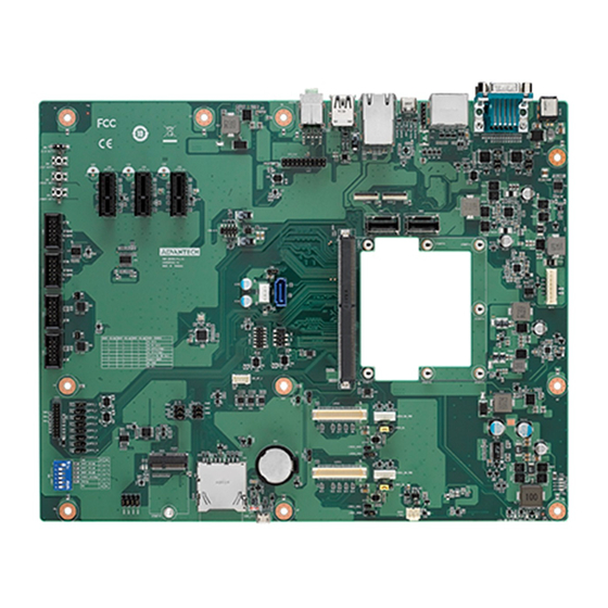
- Page 18 The operating temperature refers to the environmental temperature for the model. Operating humidity: 0% ~ 90% relative humidity, non-condensing Storage temperature: -40~85° C Relative humidity: 95% Weight (g): 80 g (weight of total package) ROM-DB5901 Looks 2.3.1 ROM-DB5901 Overview 2.3.2 I/O Connectors ROM-DB5901 User Manual...
- Page 19 HDMI Port CN33 Type C Controller Programming Header (Reserved Only) CN34 USB Type C GbE Ethernet Connector Port USB Port 1/ 2 Audio1 MIC Input/ Audio Output Table 2.2: DCIN1 (DC-Jack, +12v Power Input) Signal Signal +12V Shield ROM-DB5901 User Manual...
- Page 20 Table 2.4: CN15B (UART2, RS232/RS422/RS485) Signal Signal 422/485TX- RS232 RXD or 422/485TX+ RS232 TXD or 422/485RX+ 422/485RX- RTS# CTS# Table 2.5: CN1A (DP) Signal Signal DP0_LAN0_+ DP0_LAN0_- DP0_LAN1_+ DP0_LAN1_- DP0_LAN2_+ DP0_LAN2_- DP0_LAN3_+ DP0_LAN3_- DP0_CONFIG_1 DP0_CONFIG_2 DP0_AUX+ DP0_AUX- DP0_HPD ROM-DB5901 User Manual...
- Page 21 Table 2.6: CN1B(HDMI) Signal Signal HDMI_D2+ HDMI_D2- HDMI_D1+ HDMI_D1- HDMI_D0+ HDMI_D0- HDMI_CK+ HDMI_CK- HDMI_CEC CTRL_CK CTRL_DAT Table 2.7: CN33 (SWD Programming Header Reserved Only) Signal Signal V3P3 CCG5_XRES CCG5_SWD_CLK CCG5_SWD_IO ROM-DB5901 User Manual...
- Page 22 USB3_D- VBUS_C SSRX-1 SSRX+1 Table 2.9: CN8 (CN8A: GbE0, CN8B: GbE1) Signal Signal GBE_MDI0+ GBE_MDI0- GBE_MDI1+ GBE_MDI1- GBE_MDI2+ GBE_MDI2- GBE_MDI3+ GBE_MDI3- GBE_CTREF GBE1_MDI0+ GBE1_MDI0- GBE1_MDI1+ GBE1_MDI1- GBE1_MDI2+ GBE1_MDI2- GBE1_MDI3+ GBE1_MDI3- GBE1_CTREF GBE1_LINK_ACT# GBE1_LINK100# GBE1_LINK1000# GBE_LINK_ACT# GBE_LINK100# GBE_LINK1000# ROM-DB5901 User Manual...
- Page 23 Table 2.10: CN3 (USB Port 1/2) Signal Signal +VBUS_USB2 USB2- USB2+ USB2_SSRX- USB2_SSRX+ USB2_SSTX- USB2_SSTX+ +VBUS_USB1 USB_D-1 USB_D+1 Table 2.11: Audio1 (Audio Output) Signal Signal MIC-IN HP_L HP_R ROM-DB5901 User Manual...
- Page 24 PCIEXPRESS 36P 180D(F) DIP PCIex1 Connector 3 2EG01817-D2D-DF Serial ATA 7P 1.27mm 180D(M) DIP CN11 SATA Connector WATM-07DBN4A3B8 WAFER 4P 2.5mm 180D(M) DIP CN12 SATA Power Connector 24W1161-04S10-01T PIN HEADER 10x2P 2.0mm 180D(M) CN22 GPIOx8 sets DIP 21N22050 ROM-DB5901 User Manual...
- Page 25 TACT SW STS-091 SMD 4P H=3.8mm SLP Button TACT SW STS-091 SMD 4P H=3.8mm Power Button TACT SW STS-091 SMD 4P H=3.8mm Micro USB 5P/0.65mm/(F)/NY9T/GFL/ USB0_OTG1 USB OTG RA/S/BK/B PIN HEADER 2x5P 2.0mm 180D(M) USB-4-5 USB Port 4, Port 5 SMD 21N22050 ROM-DB5901 User Manual...
- Page 26 2.4.3 Connectors Table 2.13: BAT1 (Lithium-ion Battery Power Input) Signal Signal BAT_TEMP BAT_ID_CN I2C_DAT_BAT I2C_CK_BAT +VBATT +VBATT Table 2.14: BH1 (RTC Battery Holder) Signal Signal BAT_RTC Table 2.15: CAN1 (CAN0 Port) Signal Signal CAN0_D- CAN0_D+ ROM-DB5901 User Manual...
- Page 27 Table 2.16: CAN2 (CAN1 Port) Signal Signal CAN1_D- CAN1_D+ Table 2.17: COM1 (COM1 Port) COM1_RX COM1_TX Table 2.18: COM3 (COM3 Port, Debug Port) Signal Signal COM3_RX COM3_TX ROM-DB5901 User Manual...
- Page 28 Table 2.19: CN4 PCIex1 Connector 1 (PCIe_C) Signal Signal +12V PCIE_C_X_PRSNT# +12V +12V +12V +12V PCIE_C_CK PCIEX_C_JTAG2 PCIE_C_DAT PCIEX_C_JTAG3 +3V3_PCIE PCIEX_C_JTAG5 PCIEX_C_JTAG1 +3V3_PCIE +3V3_PCIE +3V3_PCIE PCIE_C_WAKE# PCIE_C_RST# Mechanical Key PCIE_C_X_REFCK+ PCIE_C_X_TX+ PCIE_C_X_REFCK- PCIE_C_X_TX- PCIE_C_X_RX+ +3V3_PCIE PCIE_C_X_RX- ROM-DB5901 User Manual...
- Page 29 Table 2.20: CN5 PCIex1 Connector 2 (PCIe_B) Signal Signal +12V PCIE_B_X_PRSNT# +12V +12V +12V +12V PCIE_B_CK PCIEX_B_JTAG2 PCIE_B_DAT PCIEX_B_JTAG3 +3V3_PCIE PCIEX_B_JTAG5 PCIEX_B_JTAG1 +3V3_PCIE +3V3_PCIE +3V3_PCIE PCIE_B_WAKE# PCIE_B_RST# Mechanical Key PCIE_B_X_REFCK+ PCIE_B_X_TX+ PCIE_B_X_REFCK- PCIE_B_X_TX- PCIE_B_X_RX+ +3V3_PCIE PCIE_B_X_RX- ROM-DB5901 User Manual...
- Page 30 +12V +12V +12V +12V PCIE_D_CK PCIEX_D_JTAG2 PCIE_D_DAT PCIEX_D_JTAG3 +3V3_PCIE PCIEX_D_JTAG5 PCIEX_D_JTAG1 +3V3_PCIE +3V3_PCIE +3V3_PCIE PCIE_D_WAKE# PCIE_D_RST# Mechanical Key PCIE_D_CK+ PCIE_D_X_TX+ PCIE_D_CK- PCIE_D_X_TX- PCIE_D_X_RX+ +3V3_PCIE PCIE_D_X_RX- Table 2.22: CN11 (SATA Connector) Signal Signal SATA_TX+ SATA_TX- SATA_RX- SATA_RX+ SATA_DOM_PIN7 ROM-DB5901 User Manual...
- Page 31 Table 2.23: CN12 (SATA Power Connector) Signal Signal +12V Table 2.24: CN22 (GPIO Pin Header) Signal Signal +V3_GPIO GPIO0_CN33 GPIO1_CN33 GPIO2_CN33 GPIO3_CN33 GPIO4_CN33 GPIO5_CN33 GPIO6_CN33 GPIO7_C GPIO8_C GPIO9_C GPIO10_CN33 GPIO11_C ROM-DB5901 User Manual...
- Page 32 GBE_MDI1- GBE1_MDI3+ GBE_MDI1+ GBE1_MDI3- GBE_CTREF GBE1_CTREF GBE_MDI0- PCIE_D_TX+ GBE_MDI0+ PCIE_D_TX- SPI0_CS1# GBE1_LINK_ACT# PCIE_D_RX+ SDIO_WP PCIE_D_RX- SDIO_CMD SDIO_CD# USB4+ SDIO_CK USB4- SDIO_PWR_EN USB3_VBUS_DET AUDIO_MCK SDIO_D0 I2S0_LRCK SDIO_D1 I2S0_SDOUT SDIO_D2 I2S0_SDIN SDIO_D3 I2S0_CK SPI0_CS0# ESPI_ALERT0# SPI0_CK ESPI_ALERT1# SPI0_DIN (TP5) ROM-DB5901 User Manual...
- Page 33 USB3_SSRX+ USB1- USB3_SSRX- USB1_EN_OC# USB3_3+ USB2+ USB3_3- USB2- USB2_EN_OC# USB2_SSTX+ USB2_SSTX- USB3_EN_OC# USB2_SSRX+ PCIE_A_RST# USB2_SSRX- USB4_EN_OC# PCIE_B_RST# PCIE_C_RST# PCIE_C_RX+ PCIE_C_RX- PCIE_C_REFCK+ PCIE_C_REFCK- PCIE_C_TX+ PCIE_C_TX- PCIE_A_REFCK+ PCIE_A_REFCK- PCIE_B_REFCK+ PCIE_B_REFCK- PCIE_A_RX+ PCIE_A_RX- PCIE_B_RX+ PCIE_B_RX- PCIE_A_TX+ PCIE_A_TX- PCIE_B_TX+ PCIE_B_TX- HDMI_D2+ ROM-DB5901 User Manual...
- Page 34 P130 SER0_RX S130 P131 SER0_RTS# S131 LVDS0_DSI0_D2+ P132 SER0_CTS# S132 LVDS0_DSI0_D2- P133 S133 LCD0_VDD_EN P134 SER1_TX S134 LVDS0_DSI0_CK+ P135 SER1_RX S135 LVDS0_DSI0_CK- P136 SER2_TX S136 P137 SER2_RX S137 LVDS0_DSI0_D3+ P138 SER2_RTS# S138 LVDS0_DSI0_D3- P139 SER2_CTS# S139 I2C_LCD_CK ROM-DB5901 User Manual...
- Page 35 S148 LID# P149 VDD_IN_3 S149 SLEEP# P150 VDD_IN_4 S150 VIN_PWR_BAD# P151 VDD_IN_5 S151 CHARGING# P152 VDD_IN_6 S152 CHARGER_PRSNT# P153 VDD_IN_7 S153 CARRIER_STBY# P154 VDD_IN_8 S154 CARRIER_PWR_ON P155 VDD_IN_9 S155 FORCE_RECOV# P156 VDD_IN_10 S156 BATLOW# S157 TEST# S158 ROM-DB5901 User Manual...
- Page 36 Table 2.26: CN26 (M.2 Key E Slot) Signal Signal 2412_DP_DN2 2412_DM_DN2 LED_OUT_WLAN# PCM_CLK M2_CK PCM_SYNC M2_CMD PCM_OUT M2_D0 PCM_IN M2_D1 LED_OUT_BT# M2_D2 M2_D3 BT_WAKE# M2_SDIO_WAKE# M2_TXD M2_SDIO_RST# Mechanical Key M2_RXD PCIE_A_TX+ M2_RTS PCIE_A_TX- M2_CTS PCIE_A_RX+ PCIE_A_RX- M2_PCIE_CK+ M2_PCIE_CK- M2_SYSCLK_R PCIE_A_D_RST# M2_PCIE_WAKE# W_DISABLE1# W_DISABLE2# ROM-DB5901 User Manual...
- Page 37 Table 2.27: CN38 (FAN Reserved) Signal Signal +12V ROM-DB5901 User Manual...
- Page 38 Table 2.28: CN39 (MIPI-CSI 1 FPC, 4-Lane) Signal Signal +V3_CAMAF_B +V3_CAMAF_B CSI1_D0+ CSI1_D0- CSI1_D1+ CSI1_D1- CSI1_D2+ CSI1_D2- CAM1_RST#_C CSI1_D3+ CSI1_D3- CSI1_CK+ CSI1_CK- I2C_CSI1_CK I2C_CSI1_DAT CAM1_PWR#_C CAM1_MCK ROM-DB5901 User Manual...
- Page 39 Table 2.29: CN40 (MIPI-CSI 0 FPC, 2-Lane) Signal Signal +V3_CAMAF_A +V3_CAMAF_A CAM0_MCK CAM0_PWR#_C I2C_CAM0_CK I2C_CSI0_DAT CSI0_CK+ CSI0_CK- CSI0_D0+ CSI0_D0- CAM0_RST#_C CSI0_D1+ CSI0_D1- ROM-DB5901 User Manual...
- Page 40 Table 2.30: CN41 (MIPI-CSI 0, Mini-SAS, 2-Lane) Signal Signal CSI0_SAS_CK- CSI0_SAS_CK+ +V1.8 +V1.8 +V12 +V12 CAM0_PWR#_C CSI0_SAS_D0- CSI0_SAS_D0+ CSI0_SAS_D1- CSI0_SAS_D1+ CAM0_X1_MCK CAM0_RST#_C I2C_CAM0_DAT_C I2C_CAM0_CK_C ROM-DB5901 User Manual...
- Page 41 CSI1_SAS_CK+ +V1.8 +V1.8 +V12 +V12 CAM1_PWR#_C CSI1_SAS_D0- CSI1_SAS_D0+ CSI1_SAS_D1- CSI1_SAS_D1+ CAM1_X1_MCK CAM1_RST#_C I2C_CAM1_DAT_C I2C_CAM1_CK_C CSI1_SAS_D2- CSI1_SAS_D2+ CSI1_SAS_D3- CSI1_SAS_D3+ Table 2.32: ESPI_CN1 (ESPI Pin Header) Signal Signal +V_ESPI ESPI_CS0#_C ESPI_CK_C ESPI_IO_0_C ESPI_IO_1_C ESPI_IO_2_C ESPI_CS1#_C ESPI_RESET#_C ESPI_IO_3_C ESPI_ALERT0#_C ESPI_ALERT1#_C ROM-DB5901 User Manual...
- Page 42 Table 2.33: I2C_GP_1 (I2C) Signal Signal I2C_GP_DAT_C I2C_GP_DAT_C +V_GP Table 2.34: I2S_CN3 (Audio Codec) Signal Signal Audio_VDDA Audio_VDDA I2S0_SDIN_C I2S0_SDOUT_C I2S0_LRCK_C I2S0_CK_C AUDIO_MCK_C Audio_I2C_CK MIC_BIAS Audio_I2C_DAT HP_R MIC_IN HP_L ROM-DB5901 User Manual...
- Page 43 Table 2.35: LVDS0 (LVDS0 / MIPI_DSI0 Shared Pin) Signal Signal +VDD_LVDS0 +VDD_LVDS_A +VDD_LVDS0 +VDD_LVDS_A LVDS0_D0- LVDS0_D0+ LVDS0_D1- LVDS0_D1+ LVDS0_D2- LVDS0_D2+ LVDS0_CK- LVDS0_CK+ I2C_LCD_CK_C I2C_LCD_DAT_C EDP0_HPD_A LVDS0_D3- LVDS0_D3+ LVDS_CTRL Table 2.36: LVDS0_BK_PWR (LVDS0 Backlight Power) Signal Signal +VDD_BKLT_LVDS0 LCD0_BKLT_EN_C LCD0_BKLT_PWM_C ROM-DB5901 User Manual...
- Page 44 Table 2.37: LVDS1 (LVDS1 / MIPI_DSI1 Shared Pin) ) Signal Signal +VDD_LVDS1 +VDD_LVDS1_A +VDD_LVDS1 +VDD_LVDS1_A LVDS1_D0- LVDS1_D0+ LVDS1_D1- LVDS1_D1+ LVDS1_D2- LVDS1_D2+ LVDS1_CK- LVDS1_CK+ I2C_LCD_CK_C I2C_LCD_DAT_C EDP1_HPD_A LVDS1_D3- LVDS1_D3+ LVDS1_CTRL Table 2.38: LVDS1_BK_PWR (LVDS1 Backlight Power) Signal Signal +VDD_BKLT_LVDS1 LCD1_BKLT_EN_C LCD1_BKLT_PWM_C ROM-DB5901 User Manual...
- Page 45 +3V_SDIO SD_CK SD_D0 SD_D1 SD_D2 Table 2.40: SPI_CN1 (SPI Pin Header) Signal Signal +V_SPI SPI0_CS0#_C SPI0_CK_C SPI0_DO_C SPI0_DIN_C SPI0_CST#_C Table 2.41: SW2 (Reset Button) Signal Signal RESET_IN# RESET_IN# Table 2.42: SW4 (SLP Button) Signal Signal SLEEP# SLEEP# ROM-DB5901 User Manual...
- Page 46 Table 2.43: SW5 (Power Button, CPU) Signal Signal POWER_BTN# POWER_BTN# Table 2.44: USB0_OTG1 (USB OTG) Signal Signal +USB_OTG_5V USB0-_X USB0+_X USB0_OTG_ID_X Table 2.45: USB-4-5 (USB Port4 & Port5 Pin Header) Signal Signal +VBUS_4 +VBUS_5 USB4-_C USB5-_C USB4+_C USB5+_C ROM-DB5901 User Manual...
- Page 47 Table 2.47: CN9 (SATA_DOM, Default (2-3)) Signal Signal SATA_DOM_PIN7 Table 2.48: CN10 (CANBus0, Default (1-2)) Signal Signal CAN0_D+ CAN0_D- Table 2.49: CN14 (CANBus1, Default (1-2)) Signal Signal CAN1_D+ CAN1_D- Table 2.50: CN17 (COM2_TERM1, Default (X)) Jumper Mode Jumper Mode COM2_TERM1 ROM-DB5901 User Manual...
- Page 48 Table 2.52: CN27 (SER0, Default (1-2)) Signal Signal UART0_RX SER0_RX M2_UART_RX Table 2.53: CN28 (SER0, Default (1-2)) Signal Signal UART0_TX SER0_TX M2_UART_TX Table 2.54: CN29 (SER0, Default(1-2)) Signal Signal UART0_RTS# SER0_RTS# M2_UART_RTS# Table 2.55: CN30 (SER0, Default(1-2)) Signal Signal UART0_CTS# SER0_CTS# M2_UART_CTS# ROM-DB5901 User Manual...
- Page 49 Table 2.58: CN44 (SDIO, Default (2-3)) Jumper Mode Jumper Mode M2_D1 SDIO_D1_X SD_D1 Table 2.59: CN45 (SDIO, Default (2-3)) Jumper Mode Jumper Mode M2_D2 SDIO_D2_X SD_D2 Table 2.60: CN46 (SDIO, Default (2-3)) Jumper Mode Jumper Mode M2_D3 SDIO_D3_X SD_D3 ROM-DB5901 User Manual...
- Page 50 Table 2.63: GPIO_0 (GPIO0, Default (2-3)) Signal Signal GPIO0_CN33 GPIO0_C CAM0_PWR# Table 2.64: GPIO_1 (GPIO1, Default (2-3)) Jumper Mode Jumper Mode GPIO1_CN33 GPIO1_C CAM1_PWR# Table 2.65: GPIO_2 (GPIO2, Default (2-3)) Jumper Mode Jumper Mode GPIO2_CN33 GPIO2_C CAM0_RST# ROM-DB5901 User Manual...
- Page 51 GPIO4_C HDA_RST# Table 2.68: GPIO_5 (GPIO5, Default(1-2)) Jumper Mode Jumper Mode GPIO5_CN33 GPIO5_C PWM_OUT Table 2.69: GPIO_6 (GPIO6, Default (1-2)) Jumper Mode Jumper Mode GPIO6_CN33 GPIO6_C TACHIN Table 2.70: GPIO_10 (GPIO10, Default(2-3)) Signal Signal GPIO10_CN33 GPIO10_C I2C_GP_INT ROM-DB5901 User Manual...
- Page 52 Table 2.71: LVDS0_BL (Default(1-2)) Signal Signal +VDD_BKLT_LVDS0 +12V Table 2.72: LVDS0_VDD1 (Default(1-2)) Signal Signal +VDD_LVDS0_SELECT Table 2.73: LVDS0_VDD2 (Default(X)) Signal Signal +VDD_LVDS0_SELECT +12V Table 2.74: LVDS1_BL (Default(1-2)) Signal Signal +VDD_BKLT_LVDS1 +12V Table 2.75: LVDS1_VDD0 (Default(1-2)) Signal Signal +VDD_LVDS1_SELECT ROM-DB5901 User Manual...
- Page 53 Carrier SATA Carrier SD Carrier eSPI (CS0#) Carrier SPI (CS0#) Module device (reserved) Remote boot (reserved) Module eMMC Flash Module SPI Table 2.79: SW3 (LID Button) Signal Signal LID# Table 2.80: SW6 (COM2 SWITCH) Signal Signal DB2_MODE_0 DB2_MODE_1 ROM-DB5901 User Manual...
- Page 54 Table 2.81: SW7 (COM0 Switch) Signal Signal DB0_MODE_0 DB0_MODE_1 2.4.6 LEDs Position Function Position Function SATA_ACT# VIN_PWR_BAD# VIN_Ready CARRIER_PWR_ON V12_Ready V5_Ready V3_Ready CARRIER_STBY# LED_OUT_WLAN# LED_OUT_BT# ROM-DB5901 User Manual...
- Page 55 Install the SMARC v2.0 module board (ROM-5720, ROM-5620, ROM-5721) to carrier board at a 30 degree angle. Press down the module board and make sure the 4 screw holes are aligned with the carrier board and adjust the 4 screws clockwise to fix them in place ROM-DB5901 User Manual...
- Page 56 ROM-DB5901 User Manual...
- Page 57 Chapter Advantech Services This chapter introduces Advan- tech design-in serviceability, tech- nical support and warranty policy for ROM-DB5901...
- Page 58 Comprehensive Document Support Design Assistance Service Advantech provides a check list for engineers to easily check their schematics and review service based on customer carrier board schematics. These services are pre- ventative and help to catch design errors before they happen. It helps saves on time and cost with regard to developing carrier boards.
- Page 59 Advantech has been involved in the industrial computer industry for many years and found that customers usually have the following questions when implementing modu- lar designs.
- Page 60 RISC COM. Design Stage When a product moves into the design stage, Advantech will supply a design guide of the carrier board for reference. The carrier board design guide provides pin defini- tions of the COM connector with limitations and recommendations for carrier board design, so customers can have a clear guideline to follow during their carrier board development.
- Page 61 RISC platforms usually have less support for ready-made drivers on the carrier board, therefore the customer has to learn from trial and error and finally get the best solution with the least effort. Advantech's team has years of experience in customer support and HW/SW development knowledge. Consequently, we can sup- port customers with professional advice and information as well as shortening devel- opment time and enabling more effective product integration.
- Page 62 (Dead-on-Arrival). The DOA Cross-Shipment excludes any shipping damage, cus- tomized and/or build-to-order products. For those products which are not DOA, the return fee to an authorized ADVANTECH repair facility will be at the customers' expense. The shipping fee for reconstructive products from ADVANTECH back to customers' sites will be at ADVANTECH's expense.
- Page 63 "Problem Description". Vague entries such as "does not work" and "failure" are not acceptable. If you are uncertain about the cause of the problem, please contact ADVANTECH's Application Engineers (AE). They may be able to find a solution that does not require sending the product for repair.
- Page 64 Product updates and tests upon the request of customers who are without war- ranty. If a product has been repaired by ADVANTECH, and within three months after such a repair the product requires another repair for the same problem, ADVANTECH will do this repair free of charge.
- Page 65 3.5.5 Custody of Products Submitted for Repair ADVANTECH will retain custody of a product submitted for repair for one month while it is waiting for return of a signed P/I or payment (A/R). If the customer fails to respond within such period, ADVANTECH will close the case automatically. ADVAN- TECH will take reasonable measures to stay in proper contact with the customer dur- ing this one month period.
- Page 66 No part of this publication may be reproduced in any form or by any means, electronic, photocopying, recording or otherwise, without prior written permis- sion of the publisher. All brand and product names are trademarks or registered trademarks of their respective companies. © Advantech Co., Ltd. 2020...
Need help?
Do you have a question about the ROM-DB5901 and is the answer not in the manual?
Questions and answers