Table of Contents
Advertisement
Quick Links
1. General description
PN5331B3HN
Near Field Communication (NFC) controller
Rev. 3.4 — 29 November 2017
157534
The PN533 is a highly integrated transceiver module for contactless communication at
13.56 MHz based on the 80C51 microcontroller core. It supports 6 different operating
modes:
•
ISO/IEC 14443A/MIFARE Reader/Writer
•
FeliCa Reader/Writer
•
ISO/IEC 14443B Reader/Writer
•
ISO/IEC 14443A/MIFARE Card MIFARE 1 KB or MIFARE 4 KB emulation
•
FeliCa Card emulation
•
ISO/IEC 18092, ECMA 340 Peer-to-Peer
The PN533 implements a demodulator and decoder for signals from
ISO/IEC 14443A/MIFARE compatible cards and transponders. The PN533 handles the
complete ISO/IEC 14443A framing and error detection (Parity & CRC).
The PN533 supports MIFARE 1 KB or MIFARE 4 KB emulation products. The PN533
supports contactless communication using MIFARE Higher transfer speeds up to
424 kbit/s in both directions.
The PN533 can demodulate and decode FeliCa coded signals. The PN533 handles the
FeliCa framing and error detection. The PN533 supports contactless communication
using FeliCa Higher transfer speeds up to 424 kbit/s in both directions.
The PN533 supports layers 2 and 3 of the ISO/IEC 14443 B Reader/Writer
communication scheme, except anticollision. This must be implemented in firmware as
well as upper layers.
In card emulation mode, the PN533 is able to answer to a Reader/Writer command either
according to the FeliCa or ISO/IEC 14443A/MIFARE card interface scheme. The PN533
generates the load modulation signals, either from its transmitter or from the LOADMOD
pin driving an external active circuit. A complete secure card functionality is only possible
in combination with a secure IC using the NFC-WI/S
Compliant to ECMA 340 and ISO/IEC 18092 NFCIP-1 Passive and Active communication
modes, the PN533 offers the possibility to communicate to another NFCIP-1 compliant
device, at transfer speeds up to 424 kbit/s.The PN533 handles the complete NFCIP-1
framing and error detection.
The PN533 transceiver can be connected to an external antenna for Reader/Writer or
Card/PICC modes, without any additional active component.
Product data sheet
COMPANY PUBLIC
2
C interface.
Advertisement
Table of Contents

Related Manuals for NXP Semiconductors PN5331B3HN


Summary of Contents for NXP Semiconductors PN5331B3HN
-
Page 1: General Description
PN5331B3HN Near Field Communication (NFC) controller Rev. 3.4 — 29 November 2017 Product data sheet 157534 COMPANY PUBLIC 1. General description The PN533 is a highly integrated transceiver module for contactless communication at 13.56 MHz based on the 80C51 microcontroller core. It supports 6 different operating modes: •... - Page 2 PN5331B3HN NXP Semiconductors Near Field Communication (NFC) controller The PN533 supports the following host interfaces: • USB 2.0 full speed interface (bus powered or non bus powered) • High Speed UART (HSU) PN533 has also a master I C interface enabling the drive on an I C peripheral (i.e.
-
Page 3: Features And Benefits
PN5331B3HN NXP Semiconductors Near Field Communication (NFC) controller 2. Features and benefits 80C51 microcontroller core with 45056 bytes ROM and 1224 bytes RAM Highly integrated demodulator and decoder Buffered output drivers to connect an antenna with minimum number of external components ... -
Page 4: Applications
PN5331B3HN NXP Semiconductors Near Field Communication (NFC) controller 3. Applications Computing application Consumer applications 4. Quick reference data Table 1. Quick reference data Symbol Parameter Conditions Unit USB Supply Voltage (USB 4.02 5.25 mode) Supply Voltage (non USB mode) V... -
Page 5: Ordering Information
PN5331B3HN NXP Semiconductors Near Field Communication (NFC) controller 5. Ordering information Table 2. Ordering information Type number Package Name Description Version PN5331B3HN/C270 HVQFN40 Heatsink Very thin Quad Flat package; 40 pins, plastic, SOT618-1 body 6 x 6 x 0.85 mm; leadless; MSL level 2. -
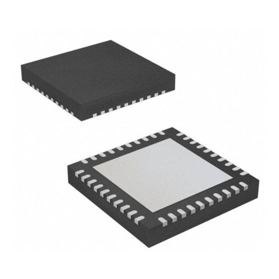
Page 6: Pinning Information
PN5331B3HN NXP Semiconductors Near Field Communication (NFC) controller 7. Pinning information 7.1 Pinning Fig 2. Pin configuration for HVQFN 40 (SOT618-1) PN5331B3HN All information provided in this document is subject to legal disclaimers. © NXP B.V. 2017. All rights reserved. -
Page 7: Pin Description
PN5331B3HN NXP Semiconductors Near Field Communication (NFC) controller 7.2 Pin description Table 3. PN533 Pin description Symbol Type Pad Ref Description Voltage DVSS Digital ground LOADMOD DVDD Load Modulation output provides digital signal for FeliCa and MIFARE card operating mode... - Page 8 PN5331B3HN NXP Semiconductors Near Field Communication (NFC) controller Table 3. PN533 Pin description …continued Symbol Type Pad Ref Description Voltage PVDD General purpose IO signal. Can be configured to act either as TX line of the second serial interface UART or general purpose IO.
-
Page 9: Functional Description
PN5331B3HN NXP Semiconductors Near Field Communication (NFC) controller 8. Functional description 8.1 80C51 The PN533 is controlled via an embedded 80C51 microcontroller core (for more details http://www.standardics.nxp.com/support/documents/microcontrollers/?scope=80C51). Its principle features are listed below: • 6-clock cycle CPU. One machine cycle comprises 6 clock cycles or states (S1 to S6). -
Page 10: Pn533 Memory Map
PN5331B3HN NXP Semiconductors Near Field Communication (NFC) controller 8.1.1 PN533 memory map The memory map of PN533 is composed of 2 main memory spaces: data memory and program memory. The following figure illustrates the structure. XRAM FFFFH FFFFH A000H BFFFH... -
Page 11: Data Memory
PN5331B3HN NXP Semiconductors Near Field Communication (NFC) controller 8.1.2 Data memory Data memory is itself divided into 2 spaces: • 384-byte IDATA with byte-wide addressing – 258-byte RAM – 128-byte SFR • 1 bank of 64 KB extended RAM (XRAM) with 2-byte-wide addressing 8.1.2.1 IDATA memory... - Page 12 xxxxxxxxxxxxxxxxxxxxx xxxxxxxxxxxxxxxxxxxxxxxxxx xxxxxxx x x x xxxxxxxxxxxxxxxxxxxxxxxxxxxxxx xxxx xxxxxxxxxxxxxxxxxxxxxxxxxxx xxxxxxxxxxxxxxxxxxx xxxxxx xxxxxxxxxxxxxxxxxxxxxxxxxxxxxxxxxxx xxxxx xxxxxxxxxxxxxxxxxxxxx xxxxxxxxxxxxxxxxxxxxxxxxxxxxxx xxxxx xxxxxxxxxxxxxxxxxxxxxxxxxxxxxxxxxxxxx xxxxxxxxxxxxxxxxxxxxxxxxx xxxxxxxxxxxxxxxxxxxx xxx Table 5. SFR map of NFC controller Address Bit- Byte-addressable addressable XRAMP P3CFGA P3CFGB P7CFGA P7CFGB CIU_Status2 CIU_FIFOData CIU_FIFOLevel CIU_WaterLevel CIU_Control CIU_BitFram CC0N...
-
Page 13: Xram Memory
PN5331B3HN NXP Semiconductors Near Field Communication (NFC) controller 8.1.2.2 XRAM memory The XRAM memory is divided into 2 memory spaces: • 0000h to 5FFFh: reserved for addressing embedded RAM. For the PN533, only accesses between 0000h and 03C7h are valid. -
Page 14: Program Memory
PN5331B3HN NXP Semiconductors Near Field Communication (NFC) controller XRAM FFFFH XRAMP = FFh XRAMP = FFh 40 kB Reserved XRAMP = 82h XRAMP = 81h XRAMP = 80h XRAMP = 7Fh XRAMP = 7Eh XRAMP = 62h XRAMP = 61h... -
Page 15: Pcon Module
PN5331B3HN NXP Semiconductors Near Field Communication (NFC) controller 8.1.4 PCON module The Power Control (PCON) module is configured using the PCON SFR register. Table 7. PCON register (SFR: address 87h) bit allocation Symbol SMOD CPU_PD Reset Access Table 8. Description of PCON bits... -
Page 16: Interrupt Enable: Ie0 And Ie1 Registers
PN5331B3HN NXP Semiconductors Near Field Communication (NFC) controller 8.1.5.2 Interrupt enable: IE0 and IE1 registers Each interrupt source can be individually enabled or disabled by setting a bit in IE0 or IE1. In register IE0, a global interrupt enable bit can be set to logic level 0 to disable all interrupts at once. -
Page 17: Interrupt Prioritization: Ip0 And Ip1 Registers
PN5331B3HN NXP Semiconductors Near Field Communication (NFC) controller The 2 following tables describe IE1. Table 12. Interrupt controller IE1 register (SFR: address E8h) bit allocation Symbol IE1_7 IE1_6 IE1_5 IE1_4 IE1_3 IE1_2 Reset Access Table 13. Description of IE1 bits... - Page 18 PN5331B3HN NXP Semiconductors Near Field Communication (NFC) controller The 2 following tables describe IP0. Table 14. Interrupt controller IP0 register (SFR: address B8h) bit allocation Symbol IP0_7 IP0_6 IP0_5 IP0_4 IP0_3 IP0_2 IP0_1 IP0_0 Reset Access Table 15. Description of IP0 bits...
-
Page 19: General Purpose Irq Control
PN5331B3HN NXP Semiconductors Near Field Communication (NFC) controller 8.1.5.4 General purpose IRQ control The general purpose interrupts are controlled by register GPIRQ. NOTE: this is not a standard feature of the 8051. Table 18. GPIRQ register (address 6107h) bit allocation... -
Page 20: Timer0/1 Description
PN5331B3HN NXP Semiconductors Near Field Communication (NFC) controller 8.1.6 Timer0/1 description Timer0/1 are general purpose timer/counters. Timer0/1 has the following functionality: • Configurable edge or level detection interrupts • Timer or counter operation • 4 timer/counter modes • Baud rate generation for Debug UART Timer0/1 comprises two 16-bit timer/counters: Timer0 and Timer1. -
Page 21: Timer0/1 Registers
PN5331B3HN NXP Semiconductors Near Field Communication (NFC) controller 8.1.6.1 Timer0/1 registers The Timer0/1 module contains six Special Function Registers (SFRs) which can be accessed by the CPU. Table 20. Timer0/1 Special Function registers list Name Size Address Description Access [bytes]... -
Page 22: T01Con Register
PN5331B3HN NXP Semiconductors Near Field Communication (NFC) controller 8.1.6.2 T01CON register The register is used to control Timer0/1 and report its status. Table 22. Timer0/1 T01CON register (SFR address 88h), bit allocation Symbol Reset Access Table 23. Description of Timer0/1 T01CON register bits... -
Page 23: T01Mod Register
PN5331B3HN NXP Semiconductors Near Field Communication (NFC) controller 8.1.6.3 T01MOD register This register is used to configure Timer0/1. Table 24. Timer 0/1 T01MOD register (SFR address 89h), bit allocation Symbol GATE1 C/T1 GATE0 C/T0 Reset Access Table 25. Description of T01MOD bits... -
Page 24: T0L And T0H Registers
PN5331B3HN NXP Semiconductors Near Field Communication (NFC) controller Table 25. Description of T01MOD bits …continued Symbol Description GATE0 Timer0 gate control. Set by firmware only. When set to logic level 1, Timer0 is enabled only when P32_INT0 is high and bit TR0 of register T01CON is set. -
Page 25: T1L And T1H Registers
PN5331B3HN NXP Semiconductors Near Field Communication (NFC) controller 8.1.6.5 T1L and T1H registers These are the actual timer/counter bytes for Timer1. T1L is the lower byte, T1H is the upper byte. Table 30. Timer0/1 T1L register (SFR address 8Bh), bit allocation Symbol T1L.7... -
Page 26: Overflow Detection
PN5331B3HN NXP Semiconductors Near Field Communication (NFC) controller 8.1.6.7 Overflow detection For both the upper and lower bytes of the Timer0/1, an overflow is detected by comparing the incremented value of the most significant bit with its previous value. An overflow... -
Page 27: T2Con Register
PN5331B3HN NXP Semiconductors Near Field Communication (NFC) controller Each increment or decrement of Timer2 occurs in state S1 except when in baud rate generation mode and configured as a counter. In this mode, Timer2 increments on each clock cycle. When configured as a timer, Timer2 is incremented every machine cycle. -
Page 28: T2Mod Register
PN5331B3HN NXP Semiconductors Near Field Communication (NFC) controller 8.1.7.3 T2MOD register This Special Function Register is used to configure Timer2. Table 37. Timer2 T2MOD register (SFR address C9h) bit allocation Symbol T2RD DCEN Reset Access Table 38. Description of TMOD bits... -
Page 29: T2L, T2H Registers
PN5331B3HN NXP Semiconductors Near Field Communication (NFC) controller 8.1.7.4 T2L, T2H registers These are the actual timer/counter bytes. T2L is the lower byte, T2H the upper byte. On the fly reading can give a wrong value since T2H can be changed after T2L is read and before T2H is read. -
Page 30: Debug Uart
PN5331B3HN NXP Semiconductors Near Field Communication (NFC) controller 8.1.8 Debug UART The Debug UART is implemented to assist debug using UART_RX and UART_TX pins. 8.1.8.1 Feature list The Debug UART has the following characteristics: • Full duplex serial port •... - Page 31 PN5331B3HN NXP Semiconductors Near Field Communication (NFC) controller • Mode 3: – 11 bits are transmitted through UART_TX or received through UART_RX: a start bit (0), 8 data bits (LSB first), a 9th data bit, and a stop bit (1). In fact, mode 3 is the same as mode 2 in all aspects except the baud rate –...
-
Page 32: S0Con Register
PN5331B3HN NXP Semiconductors Near Field Communication (NFC) controller 8.1.8.3 S0CON register The Special Function Register S0CON is the control and status register of the Debug UART. This register contains the mode selection bits (SM2, SM1, SM0), the 9th data bit for transmit and receive (TB8 and RB8), and the serial port interrupt bits (TI and RI). - Page 33 PN5331B3HN NXP Semiconductors Near Field Communication (NFC) controller Table 49. Description of S0CON bits …continued Symbol Description Receive data bit. Set by hardware and by firmware. When set to logic level 1: In modes 2 or 3, the hardware stores the 9th data bit that was received in RB8 In mode 1, the hardware stores the stop bit that was received in RB8 In mode 0, the hardware does not change RB8.
-
Page 34: S0Buf Register
PN5331B3HN NXP Semiconductors Near Field Communication (NFC) controller 8.1.8.4 S0BUF register This register is implemented twice. Writing to S0BUF writes to the transmit buffer. Reading from S0BUF reads from the receive buffer. Only hardware can read from the transmit buffer and write to the receive buffer. -
Page 35: Mode 1 And 3 Baud Rates
PN5331B3HN NXP Semiconductors Near Field Communication (NFC) controller 8.1.8.7 Mode 1 and 3 baud rates In modes 1 and 3, the baud rates are determined by the rate of timer1 and timer2 overflow bits: ‘t1_ovf’ and ‘t2_ovf’. The register bit TCLK0 from the register T2CON selects if ‘t1_ovf’... - Page 36 PN5331B3HN NXP Semiconductors Near Field Communication (NFC) controller When rewriting this formula, the value for the Timer1 reload value T1H is calculated from the desired baud rate as follows: Timer1 reload value T1H SMOD --------------------------------------------- - – ...
-
Page 37: Baud Rates Using Timer2 (Debug Uart Mode 1 And 3)
PN5331B3HN NXP Semiconductors Near Field Communication (NFC) controller 8.1.8.9 Baud rates using Timer2 (Debug UART mode 1 and 3) Timer2 has a programming mode to function as baud rate generator for the Debug UART. In this mode the baud rate is given by formula:... - Page 38 PN5331B3HN NXP Semiconductors Near Field Communication (NFC) controller At maximum 4 different controllable modes can be supported. These modes are defined with the following bits: • PxCFGA[n]=0 and PxCFGB[n]=0: Open drain • PxCFGA[n]=1 and PxCFGB[n]=0: Quasi Bidirectional (Reset mode) •...
-
Page 39: Pad Configurations Description
PN5331B3HN NXP Semiconductors Near Field Communication (NFC) controller 8.2.1 Pad configurations description 8.2.1.1 Open-drain DVDD xVDD “0” e_pu e_hd “0” PxCFGA[n] = GPIO pad “0” PxCFGB[n] = Control en_n Px[n] CPU_CLK output mode input mode CPU_CLK CPU_CLK Write Px[n] GPIO pad... -
Page 40: Quasi Bidirectional
PN5331B3HN NXP Semiconductors Near Field Communication (NFC) controller 8.2.1.2 Quasi Bidirectional DVDD xVDD Control e_pu e_hd “1” PxCFGA[n] = GPIO pad “0” PxCFGB[n] = en_n Px[n] CPU_CLK output mode input mode CPU_CLK CPU_CLK Write Px[n] GPIO pad “1” en_n en_n pushpull “0”... -
Page 41: Input
PN5331B3HN NXP Semiconductors Near Field Communication (NFC) controller 8.2.1.3 Input DVDD xVDD “0” e_pu e_hd “0” PxCFGA[n] = “1” GPIO pad PxCFGB[n] = Control en_n “1” Px[n] CPU_CLK input mode CPU_CLK GPIO pad Read Px[n] Fig 8. Input In input configuration, no pull up or hold resistor are internally connected to the pad. -
Page 42: Push-Pull Output
PN5331B3HN NXP Semiconductors Near Field Communication (NFC) controller 8.2.1.4 Push-pull output DVDD xVDD Control e_pu “0” e_hd “1” PxCFGA[n] = GPIO pad “1” PxCFGB[n] = en_n Data Px[n] CPU_CLK output mode CPU_CLK Write Px[n] en_n GPIO pad Fig 9. Push-pull output In push-pull output, the output pin drives a strong logic level 0 or a logic level 1 continuously. -
Page 43: Gpio Registers Description
PN5331B3HN NXP Semiconductors Near Field Communication (NFC) controller 8.2.2 GPIO registers description 8.2.2.1 P7CFGA register Table 60. P7CFGA register (SFR: address F4h) bit allocation Symbol P7CFGA[0] Reset Access Table 61. Description of P7CFGA bits Symbol Description 7 to 1 Reserved. -
Page 44: P3Cfga Register
PN5331B3HN NXP Semiconductors Near Field Communication (NFC) controller 8.2.2.4 P3CFGA register Table 66. P3CFGA Register (SFR: address FCh) bit allocation Symbol P3CFGA[5] P3CFGA[4] P3CFGA[3] P3CFGA[2] P3CFGA[1] P3CFGA[0] Reset Access Table 67. Description of P3CFGA Register bits Bit Symbol Description Reserved. -
Page 45: P3 Register
PN5331B3HN NXP Semiconductors Near Field Communication (NFC) controller 8.2.2.6 P3 register Table 70. P3 register (SFR: address B0h) bit allocation Symbol P3[5] P3[4] P3[3] P3[2] P3[1] P3[0] Reset Access Table 71. Description of P3 bits Symbol Description 7 to 6 Reserved. -
Page 46: P5 Register
PN5331B3HN NXP Semiconductors Near Field Communication (NFC) controller 8.2.2.7 P5 register Table 72. P5 register (SFR: address D7h) bit allocation Symbol P5[2] P5[1] P5[0] Reset Access Table 73. Description of P5 bits Symbol Description 7 to 3 Reserved. P5[2] Bit 2 of P5 register is attached to USB signal “MP_ready” that indicates USB block is ready for a new transaction like write command, write data or read data. -
Page 47: Matx Description
PN5331B3HN NXP Semiconductors Near Field Communication (NFC) controller 8.3.1 MATX description After every Power-On or Hard Reset (RSTPD_N at low level), the PN533 also resets its interfaces and checks the current HOST interface type. The PN533 identifies the selected HOST interface by means of the logic levels on the control pins I0 and I1 after the Reset Phase. -
Page 48: C Interface
PN5331B3HN NXP Semiconductors Near Field Communication (NFC) controller 8.3.2 I C interface It is recommended to refer the I C standard for more information. The I C interface implements a Master I C bus interface with integrated shift register, shift timing generation. -
Page 49: Master Transmitter Mode
PN5331B3HN NXP Semiconductors Near Field Communication (NFC) controller 8.3.2.2 Master transmitter mode As a Master, the I C logic will generate all of the serial clock pulses and the START and STOP conditions. A transfer is ended with a STOP condition or with a repeated START condition. -
Page 50: Master Receiver Mode
PN5331B3HN NXP Semiconductors Near Field Communication (NFC) controller 8.3.2.3 Master receiver mode As a Master, the I C logic will generate all of the serial clock pulses and the START and STOP conditions. A transfer is ended with a STOP condition or with a repeated START condition. - Page 51 PN5331B3HN NXP Semiconductors Near Field Communication (NFC) controller Table 79. Description of I CCON bits Symbol Description CR[2] Serial clock frequency selection in Master mode. Together with CR[1:0], this bit determines the clock rate (serial clock frequency) when the I C interface is in a Master mode.
- Page 52 PN5331B3HN NXP Semiconductors Near Field Communication (NFC) controller Table 79. Description of I CCON bits …continued Symbol Description Serial interrupt flag. When SI is set to logic level 1, then if the serial interrupt from the I C interface port is enabled, the CPU will receive an interrupt. SI is set by hardware when any one of 25 of the possible 26 states of the I C interface are entered.
- Page 53 PN5331B3HN NXP Semiconductors Near Field Communication (NFC) controller Table 79. Description of I CCON bits …continued Symbol Description 1 to 0 CR[1:0] Serial clock frequency selection in Master mode. CR2 CR1 CR0 CPU_CLK division factor I2C bit frequency CPU_CLK/10 CPU_CLK/20...
-
Page 54: Csta Register
PN5331B3HN NXP Semiconductors Near Field Communication (NFC) controller 8.3.2.5 I CSTA register CSTA is an 8-bit read-only special function register. The three least significant bits are always at logic 0. The five most significant bits contain the status code. There are 26 possible status codes. - Page 55 xxxxxxxxxxxxxxxxxxxxx xxxxxxxxxxxxxxxxxxxxxxxxxx xxxxxxx x x x xxxxxxxxxxxxxxxxxxxxxxxxxxxxxx xxxx xxxxxxxxxxxxxxxxxxxxxxxxxxx xxxxxxxxxxxxxxxxxxx xxxxxx xxxxxxxxxxxxxxxxxxxxxxxxxxxxxxxxxxx xxxxx xxxxxxxxxxxxxxxxxxxxx xxxxxxxxxxxxxxxxxxxxxxxxxxxxxx xxxxx xxxxxxxxxxxxxxxxxxxxxxxxxxxxxxxxxxxxx xxxxxxxxxxxxxxxxxxxxxxxxx xxxxxxxxxxxxxxxxxxxx xxx Table 82. C Master Transmitter Mode status code Status Status of the I C Bus Application firmware Response Next Action Taken By the I C interface H Code and of the...
- Page 56 xxxxxxxxxxxxxxxxxxxxx xxxxxxxxxxxxxxxxxxxxxxxxxx xxxxxxx x x x xxxxxxxxxxxxxxxxxxxxxxxxxxxxxx xxxx xxxxxxxxxxxxxxxxxxxxxxxxxxx xxxxxxxxxxxxxxxxxxx xxxxxx xxxxxxxxxxxxxxxxxxxxxxxxxxxxxxxxxxx xxxxx xxxxxxxxxxxxxxxxxxxxx xxxxxxxxxxxxxxxxxxxxxxxxxxxxxx xxxxx xxxxxxxxxxxxxxxxxxxxxxxxxxxxxxxxxxxxx xxxxxxxxxxxxxxxxxxxxxxxxx xxxxxxxxxxxxxxxxxxxx xxx Table 82. C Master Transmitter Mode status code …continued Status Status of the I C Bus Application firmware Response Next Action Taken By the I C interface H Code and of the...
- Page 57 xxxxxxxxxxxxxxxxxxxxx xxxxxxxxxxxxxxxxxxxxxxxxxx xxxxxxx x x x xxxxxxxxxxxxxxxxxxxxxxxxxxxxxx xxxx xxxxxxxxxxxxxxxxxxxxxxxxxxx xxxxxxxxxxxxxxxxxxx xxxxxx xxxxxxxxxxxxxxxxxxxxxxxxxxxxxxxxxxx xxxxx xxxxxxxxxxxxxxxxxxxxx xxxxxxxxxxxxxxxxxxxxxxxxxxxxxx xxxxx xxxxxxxxxxxxxxxxxxxxxxxxxxxxxxxxxxxxx xxxxxxxxxxxxxxxxxxxxxxxxx xxxxxxxxxxxxxxxxxxxx xxx Table 83. C Master Receiver Mode status codes …continued Status Status of the I C Bus and Application firmware Response Next Action Taken By the I C interface H Code...
-
Page 58: Cdat Register
PN5331B3HN NXP Semiconductors Near Field Communication (NFC) controller 8.3.2.6 I CDAT register CDAT contains a byte of I C data to be transmitted or a byte which has just been received. The CPU can read from and write to this 8-bit SFR while it is not in the process of shifting a byte. -
Page 59: I 2 Cadr Register
PN5331B3HN NXP Semiconductors Near Field Communication (NFC) controller 8.3.2.7 I CADR register The CPU can read from and write to this 8-bit SFR. I CADR is not affected by the I interface hardware. The content of this register is irrelevant when the I C interface is in a Master mode. -
Page 60: Fifo Manager
PN5331B3HN NXP Semiconductors Near Field Communication (NFC) controller 8.3.3 FIFO manager This block is designed to manage a RAM as a FIFO in order to optimize the data exchange between the CPU and the HOST. 8.3.3.1 FIFO manager functional description The RAM used for the FIFO is shared between the SPI and HSU interfaces. -
Page 61: Rwl Register
PN5331B3HN NXP Semiconductors Near Field Communication (NFC) controller Table 91. Fifo manager SFR register list Name Size Description Access [bytes] Address FIFO Receive Waterlevel: Controls the threshold of the FIFO in reception FIFO Transmit Waterlevel: Controls the threshold of the... -
Page 62: Fifofs Register
PN5331B3HN NXP Semiconductors Near Field Communication (NFC) controller 8.3.3.4 FIFOFS register This register indicates the number of bytes that the CPU can still load into the FIFO until the Transmit FIFO is full. Table 96. FIFOFS register (SFR: address 9Ch) bit allocation... -
Page 63: Sff Register
PN5331B3HN NXP Semiconductors Near Field Communication (NFC) controller 8.3.3.6 SFF register The register bits are used to allow the CPU to monitor the status of the FIFO. The primary purpose is to detect completion of data transfers. Table 100. SFF register (SFR: address 9Eh) bit allocation... -
Page 64: Fit Register
PN5331B3HN NXP Semiconductors Near Field Communication (NFC) controller 8.3.3.7 FIT register The FIT register contains 6 read-write bits which are logically OR-ed to generate an interrupt going to the CPU. Table 102. FIT register (SFR: address 9Fh) bit allocation Symbol... -
Page 65: Fiten Register
PN5331B3HN NXP Semiconductors Near Field Communication (NFC) controller 8.3.3.8 FITEN register The FITEN register enables or disables the interrupt requests to the CPU. It is also used to reset the content of the Receive and Transmit FIFO. Table 104. FITEN register (SFR: address A1h) bit allocation... -
Page 66: Fdata Register
PN5331B3HN NXP Semiconductors Near Field Communication (NFC) controller 8.3.3.9 FDATA register The FDATA register is used to provide the transmitted and received data bytes. Each data written in the data register is pushed into the Transmit FIFO. Each data read from the data register is popped from the Receive FIFO. -
Page 67: High Speed Uart (Hsu)
PN5331B3HN NXP Semiconductors Near Field Communication (NFC) controller 8.3.4 High Speed UART (HSU) The High Speed UART (HSU) provides a high speed link to the host (up to 1.288 Mbit/s). The HSU is a full duplex serial port. The serial port has a Receive-buffer: in conjunction with the FIFO manager, the reception of several bytes can be performed without strong CPU real time constraints. - Page 68 PN5331B3HN NXP Semiconductors Near Field Communication (NFC) controller tx_data hsu_txout Shift Register tx_shift tr_req TX Control CPU Interface tr_ack tx_clk hsu_tx_control HSU_STA hsu_tx_status Baud rate Prescaler Generator HSU_CTR Baud rate_control HSU_PRE hsu_rcv_status hsu_rcv_control HSU_CNT Preamble rcv_req_o rcv_req_i Filter 00 00 FF...
-
Page 69: Mode Of Operation
PN5331B3HN NXP Semiconductors Near Field Communication (NFC) controller 8.3.4.1 Mode of operation The HSU supports only one operational mode, which has the following characteristics: • Start bit: – Start bit is detected when a logic level 0 is asserted on the HSU_RX line. -
Page 70: Hsu_Sta Register
PN5331B3HN NXP Semiconductors Near Field Communication (NFC) controller 8.3.4.5 HSU_STA register The SFR HSU_STA is the status register of the HSU. Table 111. HSU_STA register (SFR: address ABh) bit allocation Symbol set_bit disable_ irq_rx_ irq_rx_fer irq_rx_ irq_rx_fer preamb over_en _ en... -
Page 71: Hsu_Ctr Register
PN5331B3HN NXP Semiconductors Near Field Communication (NFC) controller 8.3.4.6 HSU_CTR register This register controls the configuration of the HSU. Table 113. HSU_CTR register (SFR: address ACh) bit allocation Symbol hsu_wu_ start_frame tx_stopbit[1:0] rx_stopbit tx_en rx_en soft_reset_n Reset Access Table 114. Description of HSU_CTR bits... -
Page 72: Hsu_Pre Register
PN5331B3HN NXP Semiconductors Near Field Communication (NFC) controller 8.3.4.7 HSU_PRE register This register is used to configure the baud rate generator prescaler.The prescaler enlarges the range of the counter (at the cost of a lower resolution). The division factor of... -
Page 73: Usb
PN5331B3HN NXP Semiconductors Near Field Communication (NFC) controller 8.3.5 USB The USB module is an USB2.0 compliant device with embedded function. Special power management features such as a clock divider and clock switch are also implemented in the device. 8.3.5.1 Features list The USB module is a USB device only supporting full speed communication scheme. -
Page 74: Resume By Host
PN5331B3HN NXP Semiconductors Near Field Communication (NFC) controller 8.3.5.3 Resume by host Resume by host in suspend state: After 3 ms of no USB activity on the bus, the device goes in suspend. About 2 ms later the device will indicate that it no longer needs the clock (Clk_Enable_N becomes inactive). -
Page 75: Remote Wake Up
PN5331B3HN NXP Semiconductors Near Field Communication (NFC) controller Resume by Host before clock is disabled: The host can decide to wake up a suspended device, before the device has switched off its main clock. The device then simply goes out of suspend. -
Page 76: Softconnect
PN5331B3HN NXP Semiconductors Near Field Communication (NFC) controller Resume by Remote Wake up before clock is disabled: Resume by Remote Wake up before clock is disabled If USB_WakeUp_N is made active before the main clock is switched off (USB_Clk_Enable_N becomes inactive), the device waits until it has been suspended for 2 ms, then wakes up and sends a resume on its upstream port. -
Page 77: Usb Embedded Firmware View
PN5331B3HN NXP Semiconductors Near Field Communication (NFC) controller 8.3.5.6 USB embedded firmware view The USB module is mapped into the XRAM memory space. It is accessible into the peripheral area on the host if internal bus. The communication between the CPU and the USB module is based on a sequence of command and data exchange. - Page 78 PN5331B3HN NXP Semiconductors Near Field Communication (NFC) controller Table 123. USB Instruction set …continued Name Recipient Coding Data Phase Function Endpoint 2 IN Read 1 byte Function Endpoint 3 IN Read 1 byte Function Endpoint 4 OUT Read 1 byte...
- Page 79 PN5331B3HN NXP Semiconductors Near Field Communication (NFC) controller Get ErrorCode: Command: FFh Data: Read 1 byte Power On Value X X X 0 0 0 0 0 ErrorCode ErrorOccured Reserved Fig 18. ErrorCode Register Note that this is a debug command and should not be used for normal operation.
- Page 80 PN5331B3HN NXP Semiconductors Near Field Communication (NFC) controller Set Device Status: Command: FEh Data: Write 1 byte The Set Device Status command changes the Device Status Register. The value of Read Only bits is ignored. Power On Value 0 0 0 0 0 0 0 0...
- Page 81 PN5331B3HN NXP Semiconductors Near Field Communication (NFC) controller Get Current Frame Number: Command: F5h Data: Read 1 or 2 byte(s) Data: Write 2 bytes Get interrupt register: Command: F4h Data: Read 2 bytes Power On Value 0 0 0 0 0 0 0 0...
- Page 82 PN5331B3HN NXP Semiconductors Near Field Communication (NFC) controller Configuration byte: Power On Value X 0 0 0 0 0 X 1 InterruptOnNAK Reserved Reserved AlwaysPLLClock Reserved Reserved Reserved Reserved Fig 22. Configuration byte • InterruptOnNAK: A ’1’ indicates that "NAKing" is reported and will generate interrupt.
- Page 83 PN5331B3HN NXP Semiconductors Near Field Communication (NFC) controller Set Endpoints Enable: Command: D8h Data: Write 2 bytes Byte 1: Power On Value 0 0 0 0 0 0 0 0 EmbFuncCtrlOutEnpdEnable EmbFuncCtrlInEnpdEnable EmbFuncEnpd1InEnable EmbFuncEnpd2InEnable EmbFuncEnpd3InEnable EmbFuncEnpd4OutEnable EmbFuncEnpd4InEnable Reserved Byte 2:...
- Page 84 PN5331B3HN NXP Semiconductors Near Field Communication (NFC) controller Get Embedded Port Status: Command: E0h Data: Read 1 byte When SuspendChange and BusReset bit are set, the appropriate bit in the interrupt register is set and an interrupt is generated to the micro-controller.
- Page 85 PN5331B3HN NXP Semiconductors Near Field Communication (NFC) controller Select Endpoint: Command: 00h - 09h Data: Read 1 byte (Optional) This command initializes an internal pointer to the start of the Selected buffer. Optionally, this command can be followed by a data read, which returns some additional info on the packet in the buffer.
- Page 86 PN5331B3HN NXP Semiconductors Near Field Communication (NFC) controller Select Endpoint/Clear Interrupt: Command: 40h - 49h Data: Read 1 byte Commands 40h to 49h are identical to their Select Endpoint equivalent, with the following differences: • The command clears the associated interrupt •...
- Page 87 PN5331B3HN NXP Semiconductors Near Field Communication (NFC) controller The data in the buffer are organized as follow: Table 126. Read buffer bytes Bit Position Byte 0 Byte 1 Number of Data bytes in buffer Byte 2 Data byte 0 Byte n+1...
- Page 88 PN5331B3HN NXP Semiconductors Near Field Communication (NFC) controller Validate Buffer: Command: FAh Data: None When the microprocessor has written data into an IN buffer, it should set the buffer full flag by the Validate Buffer command. This indicates that the data in the buffer is valid and can be sent to the host when the next IN token is received.
-
Page 89: Power Management
PN5331B3HN NXP Semiconductors Near Field Communication (NFC) controller 8.4 Power management This chapter defines the power distribution scheme according to the different system configuration. The PN533 can be supplied by the USB connector on VBUS or directly on the VBUS, AVDD, DVDD, PVDD and TVDD. Regarding the system configuration (USB BUS powered, USB non bus powered or HOST powered), the power distribution shall be different. -
Page 90: Usb Non Bus Powered
PN5331B3HN NXP Semiconductors Near Field Communication (NFC) controller 8.4.2 USB non bus powered In this mode, the power distribution can be either HOST powered single source or HOST powered double source as described in Section 8.4.3 “HOST powered (single source)”... -
Page 91: Host Powered (Double Source)
PN5331B3HN NXP Semiconductors Near Field Communication (NFC) controller 8.4.4 HOST powered (double source) The power distribution is performed from the second source from the Host. The Figure 32 “HOST powered from double source” depicts the system approach for the power distribution. -
Page 92: Low Power Modes
PN5331B3HN NXP Semiconductors Near Field Communication (NFC) controller 8.4.5 Low power modes There are 2 different low power modes. • “Hard power-down” controlled by the pin RSTPD_N. In that case, the PN533 enters into the reset state and the maximum consumption depends on the connection of PN533 to the USB bus or not. -
Page 93: Regulator - Short Description
PN5331B3HN NXP Semiconductors Near Field Communication (NFC) controller 8.4.7 Regulator - short description The regulator is used to reduce the VBUS voltage to the typical operating voltage of PN533. VBUS Fig 33. 3.3 V regulator block diagram The 3.3V regulator is a linear regulator with resistive feed-back. The regulator uses the Band-gap for reference voltage 8.4.8 Main switch... -
Page 94: Svdd Switch
PN5331B3HN NXP Semiconductors Near Field Communication (NFC) controller 8.4.9 SVDD switch The SVDD switch is used to control power to the secure IC. The switch is controlled by register Control_switch_rng (address 6106h). The switch is enabled with bit sic_switch_en. When disabled, the SVDD pin is tied to ground. A current limiter is incorporated into the switch. -
Page 95: Power Clock And Reset Controller
PN5331B3HN NXP Semiconductors Near Field Communication (NFC) controller 8.5 Power clock and reset controller The PCR controller is the controller for the clock generation, power management and reset architecture for the PN533. 8.5.1 PCR in the system This block diagram Figure 34 “PN533 Power Management block diagram”... - Page 96 PN5331B3HN NXP Semiconductors Near Field Communication (NFC) controller INT0 CPU 80C51 Data/Control USB_INT CLK96_GEN STATUS & CONTROL registers PLL_CLK96 Gating PLL_LOCK p32_int0 p33_int1 PLL_EN GPIRQ CLK27_GEN bit enable OSC27_STABLE %1,2,4 OSC27_CLK Selection CPU_CLK OSC27_EN 27.12MHz PCR_wakeup PCR_int0 Gating SYS_RESET_N POWER_SEQ...
-
Page 97: Mhz Crystal Oscillator
PN5331B3HN NXP Semiconductors Near Field Communication (NFC) controller 8.5.2 27.12 MHz crystal oscillator The 27.12 MHz clock applied to the PN533 is the time reference for the embedded microcontroller. Therefore stability of the clock frequency is an important factor for reliable operation. -
Page 98: Power-Up Sequence
PN5331B3HN NXP Semiconductors Near Field Communication (NFC) controller 8.5.4 Power-up sequence In a USB application, the embedded firmware shall start the USB PLL. The embedded firmware shall follow below sequence: • Configure MATX in USB mode. • Enable 96MHz PLL by setting PLL_en bit of PCR control register (6203h) to logic level 1. -
Page 99: Reset Modes
PN5331B3HN NXP Semiconductors Near Field Communication (NFC) controller 8.5.6 Reset modes The possible reset mechanisms are listed below: • Supply rail variation When DVDD falls below Vth, the POR (Power-On-Reset) asserts an internal reset signal. The Power Sequencer disables all clocks. When DVDD rises above Vth+Vhys, the POR deasserts the internal reset signal and the Power Sequencer starts the power-up sequence. -
Page 100: Suspend Mode
PN5331B3HN NXP Semiconductors Near Field Communication (NFC) controller 8.5.8 Suspend mode After 3 ms of no USB activity on the bus, the device goes in suspend. About 2 ms later the device will indicate that it no longer needs the clock by setting to logic level one suspended bit (refer to bit “suspended”... -
Page 101: Remote Wake-Up
PN5331B3HN NXP Semiconductors Near Field Communication (NFC) controller 8.5.9 Remote wake-up The PN533 can be woken up from a Soft-Power-down mode or Suspend mode when an event occurs on one of the wake up sources, which has been enabled. There are seven wake-up sources: •... -
Page 102: Pcr Extension Registers
PN5331B3HN NXP Semiconductors Near Field Communication (NFC) controller 8.5.10 PCR extension registers The PCR is controlled via several registers given in Table 133: Table 133. PCR registers Name Size [bytes] Address offset Description Reset 6200h Clock Frequency Register 6201h Clock Enable Register... -
Page 103: Cer Register
PN5331B3HN NXP Semiconductors Near Field Communication (NFC) controller 8.5.11.2 CER register The Clock Enable Register is used to enable or disable the clock of the USB and HSU interfaces (frequency is fixed at 27.12 MHz). The clock can be switched on or off at any time. -
Page 104: Ilr Register
PN5331B3HN NXP Semiconductors Near Field Communication (NFC) controller 8.5.11.3 ILR register The Interrupt Level Register is used to program the level of the external interrupts. Firmware can write to this register at any time. Table 138. PCR ILR register (address 6202h) bit allocation... -
Page 105: Pcr Control Register
PN5331B3HN NXP Semiconductors Near Field Communication (NFC) controller 8.5.11.4 PCR Control register The Control register is used to perform a firmware reset and clear wake-up conditions in the Status register. Table 140. PCR Control register (address 6203h) bit allocation Symbol... -
Page 106: Pcr Status Register
PN5331B3HN NXP Semiconductors Near Field Communication (NFC) controller 8.5.11.5 PCR Status register The PCR Status register stores the state of the 7 wake-up events, reported within 6 flags. Table 142. PCR Status register (address 6204h) bit allocation Symbol gpirq_wu HSU_wu... -
Page 107: Wakeupen Register
PN5331B3HN NXP Semiconductors Near Field Communication (NFC) controller 8.5.11.6 Wakeupen register Register Wakeupen allows the selection of different wake-up events. Table 144. PCR Wakeupen register (address 6205h) bit allocation Symbol GPIRQ_ HSU_on_ CIU_wu_ clock_on_ int1_en int0_en wu_en Reset Access Table 145. Description of PCR Wakeupen bits... -
Page 108: Contactless Interface Unit (Ciu)
PN5331B3HN NXP Semiconductors Near Field Communication (NFC) controller 8.6 Contactless Interface Unit (CIU) The PN533 CIU is a modem for contactless communication at 13.56 MHz. It supports 6 different operating modes • ISO/IEC 14443A/MIFARE Reader/Writer • FeliCa Reader/Writer • ISO/IEC 14443B Reader/Writer •... -
Page 109: Feature List
PN5331B3HN NXP Semiconductors Near Field Communication (NFC) controller 8.6.1 Feature list • Frequently accessed registers placed in SFR space • Highly integrated analog circuitry to demodulate and decode received data • Buffered transmitter drivers to minimize external components to connect an antenna. -
Page 110: Simplified Block Diagram
PN5331B3HN NXP Semiconductors Near Field Communication (NFC) controller 8.6.2 Simplified block diagram PN533 80C51 Data Mode Detector Serial FIFO Level Data CL UART Detector Switch Analog Interface Contactless Interface Unit Fig 38. Simplify Contactless Interface Unit (CIU) block diagram The Analog Interface handles the modulation and demodulation of the analog signals according to the Card emulation mode, Reader/Writer mode and NFCIP-1 mode communication scheme. -
Page 111: Reader/Writer Modes
PN5331B3HN NXP Semiconductors Near Field Communication (NFC) controller 8.6.3 Reader/Writer modes All indicated modulation indices and modes in this chapter are system parameters. This means that beside the IC settings a suitable antenna tuning is required to achieve the optimal performance. - Page 112 PN5331B3HN NXP Semiconductors Near Field Communication (NFC) controller Fig 40. Data coding and framing according to ISO/IEC 14443A PN5331B3HN All information provided in this document is subject to legal disclaimers. © NXP B.V. 2017. All rights reserved. Product data sheet Rev.
-
Page 113: Felica Reader/Writer
PN5331B3HN NXP Semiconductors Near Field Communication (NFC) controller 8.6.3.2 FeliCa Reader/Writer The following diagram describes the communication at the physical level. Table 147 describes the physical parameters. 1. Reader/Writer to Card 8 - 30% ASK, Manchester Coded, Baud rate 212 to 424 kbit/s... -
Page 114: Iso/Iec 14443B Reader/Writer
PN5331B3HN NXP Semiconductors Near Field Communication (NFC) controller 8.6.3.3 ISO/IEC 14443B Reader/Writer The CIU supports layers 2 and 3 of the ISO/IEC 14443B Reader/Writer communication scheme, except anticollision which must be implemented in firmware as well as upper layers. The following diagram describes the communication at the physical level. -
Page 115: Iso/Iec 18092, Ecma 340 Nfcip-1 Operating Mode
PN5331B3HN NXP Semiconductors Near Field Communication (NFC) controller 8.6.4 ISO/IEC 18092, ECMA 340 NFCIP-1 operating mode A NFCIP-1 communication takes place between 2 devices: • Initiator: generates RF field at 13.56 MHz and starts the NFCIP-1 communication. • Target: responds to initiator command either in a load modulation scheme in Passive Communication mode or using a self generated and self modulated RF field for Active Communication mode. -
Page 116: Active Communication Mode
PN5331B3HN NXP Semiconductors Near Field Communication (NFC) controller 8.6.4.1 ACTIVE Communication mode Active Communication Mode means both the Initiator and the Target are using their own RF field to transmit data. Host Host 1. Initiator starts the communication PN533 PN533... -
Page 117: Passive Communication Mode
PN5331B3HN NXP Semiconductors Near Field Communication (NFC) controller 8.6.4.2 PASSIVE Communication mode Passive Communication Mode means that the target answers to an Initiator command in a load modulation scheme. Host Host 1. Initiator starts communication PN533 PN533 at selected transfer speed... -
Page 118: Nfcip-1 Framing And Coding
PN5331B3HN NXP Semiconductors Near Field Communication (NFC) controller 8.6.4.3 NFCIP-1 framing and coding The NFCIP-1 framing and coding in Active and Passive communication modes are defined in the NFCIP-1 standard: ISO/IEC 18092 or ECMA 340. 8.6.4.4 NFCIP-1 protocol support The NFCIP-1 protocol is not completely described in this document. For detailed explanation of the protocol refer to the ISO/IEC 18092 / ECMA340 NFCIP-1 standard. -
Page 119: Card Operating Modes
PN5331B3HN NXP Semiconductors Near Field Communication (NFC) controller 8.6.5 Card operating modes The PN533 can be addressed like a FeliCa or ISO/IEC 14443A/MIFARE card. This means that the PN533 can generate an answer in a load modulation scheme according to the ISO/IEC 14443A/MIFARE or FeliCa interface description. - Page 120 PN5331B3HN NXP Semiconductors Near Field Communication (NFC) controller Table 153. Communication overview for ISO/IEC 14443A/MIFARE Card operating mode Communication scheme ISO/IEC 14443A MIFARE higher baud rate MIFARE Baud rate 106 kbit/s 212 kbit/s 424 kbit/s ------------------------- - ------------------------- - 9,44s...
-
Page 121: Felica Card Operating Mode
PN5331B3HN NXP Semiconductors Near Field Communication (NFC) controller 8.6.5.2 FeliCa Card operating mode With appropriate firmware, the PN533 can handle the FeliCa protocol. The following diagram describes the communication at the physical level. Table 154 describes the physical parameters. 1. Reader/Writer to Card 8 - 30% ASK,... - Page 122 PN5331B3HN NXP Semiconductors Near Field Communication (NFC) controller PN533 80C51 State Machine Control Register bank CIU_Command register Programmable timer CIU FIFO control CIU FIFO control CIU interrupt control CIU 64-byte FIFO CRC16 generation & check MIFARE Classic unit Random Number Generator...
-
Page 123: Transmitter Control
PN5331B3HN NXP Semiconductors Near Field Communication (NFC) controller 8.6.7 Transmitter control The signals delivered by the transmitter are on pins TX1 and pin TX2. The supply and grounds of the transmitter drivers are TVDD, TVSS1 and TVSS2. The signals delivered are the 13.56 MHz energy carrier modulated by an envelope signal. - Page 124 xxxxxxxxxxxxxxxxxxxxx xxxxxxxxxxxxxxxxxxxxxxxxxx xxxxxxx x x x xxxxxxxxxxxxxxxxxxxxxxxxxxxxxx xxxx xxxxxxxxxxxxxxxxxxxxxxxxxxx xxxxxxxxxxxxxxxxxxx xxxxxx xxxxxxxxxxxxxxxxxxxxxxxxxxxxxxxxxxx xxxxx xxxxxxxxxxxxxxxxxxxxx xxxxxxxxxxxxxxxxxxxxxxxxxxxxxx xxxxx xxxxxxxxxxxxxxxxxxxxxxxxxxxxxxxxxxxxx xxxxxxxxxxxxxxxxxxxxxxxxx xxxxxxxxxxxxxxxxxxxx xxx Table 155. Settings for TX1 Force InvTx1 InvTx1 Envelope TX1 GsPMos GsNMos Remarks RFEn 100ASK RFON RFOFF ModGsNOff If TX1RFEN is set to logic level 0, the pin TX1 is on InvTx1RFOFF.
- Page 125 xxxxxxxxxxxxxxxxxxxxx xxxxxxxxxxxxxxxxxxxxxxxxxx xxxxxxx x x x xxxxxxxxxxxxxxxxxxxxxxxxxxxxxx xxxx xxxxxxxxxxxxxxxxxxxxxxxxxxx xxxxxxxxxxxxxxxxxxx xxxxxx xxxxxxxxxxxxxxxxxxxxxxxxxxxxxxxxxxx xxxxx xxxxxxxxxxxxxxxxxxxxx xxxxxxxxxxxxxxxxxxxxxxxxxxxxxx xxxxx xxxxxxxxxxxxxxxxxxxxxxxxxxxxxxxxxxxxx xxxxxxxxxxxxxxxxxxxxxxxxx xxxxxxxxxxxxxxxxxxxx xxx Table 156. Settings for TX2 …continued Force TX2CW InVTx2 InvTx2 Envelope TX2 GsPMos GsNMos Remarks RFEn 100ASK RFON RFOFF ModGsP ModGsNOn When TX2RFEn is set to logic level 1 an level 0, the phase of TX2 is depending on CWGsP CWGsNOn...
-
Page 126: Rf Level Detector
PN5331B3HN NXP Semiconductors Near Field Communication (NFC) controller 8.6.8 RF level detector The RF level detector is integrated to fulfill NFCIP-1 protocol requirements (e.g. RF collision avoidance). Furthermore the RF level detector can be used to wake up the PN533 and to generate an interrupt. -
Page 127: Antenna Presence Self Test
PN5331B3HN NXP Semiconductors Near Field Communication (NFC) controller 8.6.9 Antenna presence self test The goal of the Antenna Presence Self Test is to facilitate at assembly phase the detection of the absence of the antenna and/or antenna matching components. Such a detection is done by mean of measuring the current consumption. -
Page 128: Antenna Presence Detector Register
PN5331B3HN NXP Semiconductors Near Field Communication (NFC) controller • Cases 1 and 2: If the antenna and/or the tuning network are not connected, the TVDD current is higher than the nominal one. The antenna detector detects this higher consumption and the andet_up bit in andet_control register is set to high •... -
Page 129: Random Generator
PN5331B3HN NXP Semiconductors Near Field Communication (NFC) controller 8.6.10 Random generator The random generator is used to generate various random number needed for the NFCIP-1 protocol, as well as for MIFARE security. It can also be used for test purpose, by generating random data through the field. -
Page 130: Data Mode Detector
PN5331B3HN NXP Semiconductors Near Field Communication (NFC) controller Table 163. Description of Control_switch_rng bits …continued Bit Symbol Description cpu_need_rng Force the random number generator in running mode. When set to logic 0, the random number generator is under control of the CIU. -
Page 131: Serial Data Switch
PN5331B3HN NXP Semiconductors Near Field Communication (NFC) controller 8.6.12 Serial data switch Two main blocks are implemented in the CIU. A digital block comprising state machines, coder and decoder logic and an analog block with the modulator and antenna drivers, receiver and amplifier. - Page 132 PN5331B3HN NXP Semiconductors Near Field Communication (NFC) controller LoadModSel Internal invert if Tristate coder INVMOD=1 LOADMOD TxMIX Envelope invert if SIGIN POLSIGN=0 LoadModTst TstBusbit Fig 52. Serial data switch for LOADMOD pin PN5331B3HN All information provided in this document is subject to legal disclaimers.
-
Page 133: Nfc-Wi/S C Interface Support
ISO/IEC 14443A signal sent by the secure IC. The SIGOUT pin can provide a digital signal and a clock to communicate to the secure IC. A secure IC can be a smart card IC provided by NXP Semiconductors. The PN533 generates the supply SVDD to the secure IC. The pins SIGIN and SIGOUT are referred to this supply, as well as pin P34 / SIC_CLK, which can be used as an extra pin for the connection to a secure IC. -
Page 134: Signal Shape For Felica Nfc-Wi/S C Interface Support
PN5331B3HN NXP Semiconductors Near Field Communication (NFC) controller 8.6.13.1 Signal shape for FeliCa NFC-WI/S C interface support The FeliCa secure IC is connected to the PN533 via the pins SIGOUT and SIGIN. The signal at SIGOUT contains the information of the 13.56 MHz clock and the digitized demodulated signal. -
Page 135: Signal Shape For Iso/Iec14443A And Mifare Nfc-Wi/S C Support
PN5331B3HN NXP Semiconductors Near Field Communication (NFC) controller 8.6.13.2 Signal shape for ISO/IEC14443A and MIFARE NFC-WI/S C support The secure IC, e.g. the SmartMX is connected to the PN533 via the pins SIGOUT, SIGIN and P34 / SIC_CLK. The signal at SIGOUT is a digital 13.56 MHz Miller coded signal between PVSS and SVDD. -
Page 136: Nfc-Wi/S C Initiator Mode
PN5331B3HN NXP Semiconductors Near Field Communication (NFC) controller 8.6.13.3 NFC-WI/S C initiator mode The PN533 includes 2 counters of 127 and 31, with digital filtering, to enable activation from the secure IC (ACT_REQ_Si), or the command to go from data to command mode (ESC_REQ). -
Page 137: Polling Sequence Functionality For Target
PN5331B3HN NXP Semiconductors Near Field Communication (NFC) controller 8.6.14.2 Polling sequence functionality for target 1. The 80C51 has to configure the CIU with the correct polling response parameters for the Polling command. 2. To activate the automatic polling in target mode, the AutoColl Command has to be activated. -
Page 138: Crc Co-Processor
PN5331B3HN NXP Semiconductors Near Field Communication (NFC) controller 8.6.15 CRC co-processor The CRC preset value of the CRC co-processor can be configured to 0000h, 6363h, A671h or FFFFh depending of the bits CRCPreset in the register Mode.This is only valid when using CalcCRC command (see Section 8.6.20.7 “CalcCRC command”... -
Page 139: Status Information About The Fifo Buffer
PN5331B3HN NXP Semiconductors Near Field Communication (NFC) controller 8.6.16.3 Status information about the FIFO buffer The 80C51may obtain the following data about the FIFO-buffers status: • Number of bytes already stored in the FIFO-buffer: FIFOLevel[6:0] in register CIU_FIFOLevel • Warning, that the FIFO-buffer is quite full: HiAlert in register CIU_Status1 •... -
Page 140: Ciu_Timer
PN5331B3HN NXP Semiconductors Near Field Communication (NFC) controller 8.6.17 CIU_timer A timer unit is implemented in the CIU: CIU_timer. The 80C51 use CIU_timer to manage timing relevant tasks for contactless communication. CIU_timer may be used in one of the following configurations: •... -
Page 141: Interrupt Request System
PN5331B3HN NXP Semiconductors Near Field Communication (NFC) controller 8.6.18 Interrupt request system The CIU indicates certain events by setting interrupt bits in the register CIU_Status1 and, in addition it will set to logic level 1 CIU_interrupt1 or CIU_IRQ_0. If this interrupt is... -
Page 142: Ciu Power Reduction Modes
PN5331B3HN NXP Semiconductors Near Field Communication (NFC) controller Table 166. High priority interrupt sources (CIU_IRQ_0) Interrupt Flag Interrupt source Set automatically, WHEN TxIRq Transmitter a transmitted data stream ends RxIRq Receiver a received data stream ends HiAlertIRq FIFO-buffer the FIFO-buffer is getting full... -
Page 143: Transmitter Power-Down
PN5331B3HN NXP Semiconductors Near Field Communication (NFC) controller 8.6.19.3 Transmitter Power-down The Transmitter Power-down mode switches off the internal antenna drivers to turn off the RF field by setting the bits Tx1RFEn and Tx2RFEn in the register CIU_TxControl to logic level 0. -
Page 144: Commands Overview
PN5331B3HN NXP Semiconductors Near Field Communication (NFC) controller 8.6.20.3 Commands overview Table 168. Command overview Command Command code Action Idle 0000 No action; cancels current command execution. Config 0001 Configures the CIU for FeliCa, MIFARE and NFCIP-1 communication. Generate RandomID 0010... -
Page 145: Config Command
PN5331B3HN NXP Semiconductors Near Field Communication (NFC) controller 8.6.20.5 Config command To configure the automatic MIFARE Anticollision, FeliCa Polling and NFCID3, the data used for these transactions have to be stored internally. All the following data have to be written to the FIFO in this order: •... -
Page 146: Transmit Command
PN5331B3HN NXP Semiconductors Near Field Communication (NFC) controller 8.6.20.8 Transmit command The content of the FIFO is transmitted immediately after starting the command. Before transmitting FIFO content, all relevant register settings have to be set to transmit data in the selected mode. -
Page 147: Autocoll Command
PN5331B3HN NXP Semiconductors Near Field Communication (NFC) controller 8.6.20.12 AutoColl command This command automatically handles the MIFARE activation and the FeliCa polling in the Card Operation mode. The bit Initiator in the CIU_Control register has to be set to logic level 0 for correct operation. - Page 148 PN5331B3HN NXP Semiconductors Near Field Communication (NFC) controller Fig 58. AutoColl command • NFCIP-1 106 kbps passive communication mode: The MIFARE anticollision is finished and the command changes automatically to Transceive. The FIFO contains the ATR_REQ frame including the start byte F0h. The bit TargetActivated in the register CIU_Status2 is set to logic 1 •...
-
Page 149: Mfauthent Command
PN5331B3HN NXP Semiconductors Near Field Communication (NFC) controller 8.6.20.13 MFAuthent command This command handles the MIFARE authentication in Reader/Writer mode to enable a secure communication to any MIFARE 1 KB and MIFARE 4 KB emulation card. The following data shall be written to the FIFO before the command can be activated: •... -
Page 150: Ciu Tests Signals
PN5331B3HN NXP Semiconductors Near Field Communication (NFC) controller 8.6.21 CIU tests signals 8.6.21.1 CIU self-test The CIU has the capability to perform a self-test. To start the self-test the following procedure has to be performed: 1. Perform a SoftReset. 2. Clear the internal buffer by writing 25 bytes of 00h and perform the Config command. -
Page 151: Ciu Test Bus
PN5331B3HN NXP Semiconductors Near Field Communication (NFC) controller 8.6.21.2 CIU test bus The test bus is implemented for production test purposes. The following configuration can be used to improve the design of a system using the PN533. The test bus allows to route internal signals to output pins. -
Page 152: Test Signals At Pin Aux
PN5331B3HN NXP Semiconductors Near Field Communication (NFC) controller 8.6.21.3 Test signals at pin AUX Each signal can be switched to pin AUX1 or AUX2 by setting SelAux1 or SelAux2 in the register CIU_AnalogTest. See Table 280 on page 195 8.6.21.4 PRBS Enables the Pseudo Random Bit Stream of 9-bit or 15-bit length sequence, PRBS9 or PRBS15, according to ITU-TO150. -
Page 153: Ciu Memory Map
PN5331B3HN NXP Semiconductors Near Field Communication (NFC) controller 8.6.22 CIU memory map The registers of the CIU are either map into the SFR or into the XRAM memory space. Table 174. Contactless Interface Unit SFR memory map ADDR Byte Register name... - Page 154 PN5331B3HN NXP Semiconductors Near Field Communication (NFC) controller Table 175. Contactless Interface Unit extension memory map …continued ADDR Byte Register name Description size 630Eh 1 CIU_TypeB Configure the ISO/IEC 14443 type B 630Fh 1 Reserved 6310h 1 Reserved 6311h 1...
-
Page 155: Ciu Register Description
PN5331B3HN NXP Semiconductors Near Field Communication (NFC) controller 8.6.23 CIU register description 8.6.23.1 CIU register bit behaviour Depending of the functionality of a register, the access condition to the bits can vary. The following table describes the access conditions: Table 176. Behavior of register bits... -
Page 156: Ciu_Command Register (D1H Or 6331H)
PN5331B3HN NXP Semiconductors Near Field Communication (NFC) controller 8.6.23.3 CIU_Command register (D1h or 6331h) Starts and stops the command execution. Table 179. CIU_Command register (address D1h or 6331h) bit allocation Symbol RcvOff Power-down Command Reset Access Table 180. Description of CIU_Command bits... -
Page 157: Ciu_Commien Register (D2H Or 6332H)
PN5331B3HN NXP Semiconductors Near Field Communication (NFC) controller 8.6.23.4 CIU_CommIEn register (D2h or 6332h) Control bits to enable and disable the passing of interrupt requests. Table 181. CIU_CommIEn register (address D2h or 6332h) bit allocation Symbol TxIEn RXIEn SiginAct IEn ModeIEn CRCIEn... -
Page 158: Ciu_Commirq Register (D4H Or 6334H)
PN5331B3HN NXP Semiconductors Near Field Communication (NFC) controller 8.6.23.6 CIU_CommIrq register (D4h or 6334h) Contains common CIU interrupt request flags. Table 185. CIU_CommIrq register (address D4h or 6334h) bit allocation Symbol Set1 TxIRq RxIRq IdleIrq HiAltertIRq LoAlertIRq ErrIRq TimerIRq Reset Access Table 186. -
Page 159: Ciu_Divirq Register (D5H Or 6335H)
PN5331B3HN NXP Semiconductors Near Field Communication (NFC) controller 8.6.23.7 CIU_DivIrq register (D5h or 6335h) Contains miscellaneous interrupt request flags. Table 187. CIU_DivIrq register (address D5h or 6335h) bit allocation Symbol Set2 SiginActIrq ModeIRq CRCIRq RfOnIRq RfOffIRq Reset Access Table 188. Description of CIU_DivIrq bits... -
Page 160: Ciu_Error Register (D6H Or 6336H)
PN5331B3HN NXP Semiconductors Near Field Communication (NFC) controller 8.6.23.8 CIU_Error register (D6h or 6336h) Error flags showing the error status of the last command executed. Table 189. CIU_Error register (address D6h or 6336h) bit allocation Symbol WrErr TempErr RFErr BufferOvfl... -
Page 161: Ciu_Status1 Register (Dfh Or 6337H)
PN5331B3HN NXP Semiconductors Near Field Communication (NFC) controller 8.6.23.9 CIU_Status1 register (DFh or 6337h) Contains status flags of the CRC, Interrupt Request System and FIFO buffer. Table 191. CIU_Status1 register (address DFh or 6337h) bit allocation Symbol CIU_IRQ_1 CRCOk CRCReady CIU_IRQ_0 TRunning RFOn HiAlert LoAlert... -
Page 162: Ciu_Status2 Register (E9H Or 6338H)
PN5331B3HN NXP Semiconductors Near Field Communication (NFC) controller 8.6.23.10 CIU_Status2 register (E9h or 6338h) Contain status flags of the receiver, transmitter and Data Mode Detector. Table 193. CIU_Status2 register (address E9h or 6338h) bit allocation Symbol TempSensClear RFFreqOK TgActivated MFCrypto1On... -
Page 163: Ciu_Fifodata Register (Eah Or 6339H)
PN5331B3HN NXP Semiconductors Near Field Communication (NFC) controller 8.6.23.11 CIU_FIFOData register (EAh or 6339h) In- and output of 64 byte FIFO buffer. Table 195. CIU_FIFOData register (address EAh or 6339h) bit allocation Symbol FIFOData[7:0] Reset Access Table 196. Description of CIU_FIFOData bits... -
Page 164: Ciu_Waterlevel Register (Ech Or 633Bh)
PN5331B3HN NXP Semiconductors Near Field Communication (NFC) controller 8.6.23.13 CIU_WaterLevel register (ECh or 633Bh) Defines the thresholds for FIFO under- and overflow warning. Table 199. CIU_WaterLevel register (address ECh or 633Bh) bit allocation Symbol WaterLevel[6:0] Reset Access Table 200. Description of CIU_WaterLevel bits... -
Page 165: Ciu_Bitframing Register (Eeh Or 633Dh)
PN5331B3HN NXP Semiconductors Near Field Communication (NFC) controller 8.6.23.15 CIU_BitFraming register (EEh or 633Dh) Adjustments for bit oriented frames. Table 203. CIU_BitFraming register (address EEh or 633Dh) bit allocation Symbol StartSend RxAlign[2:0] TxLastBits[2:0] Reset Access Table 204. Description of CIU_BitFraming bits... -
Page 166: Ciu_Coll Register (Efh Or 633Eh)
PN5331B3HN NXP Semiconductors Near Field Communication (NFC) controller 8.6.23.16 CIU_Coll register (EFh or 633Eh) Defines the first bit collision detected on the RF interface. Table 205. CIU_Coll register (address EFh or 633Eh) bit allocation Symbol ValuesAfterColl CollPosNotValid CollPos Reset Access Table 206. -
Page 167: Ciu_Mode Register (6301H)
PN5331B3HN NXP Semiconductors Near Field Communication (NFC) controller 8.6.23.17 CIU_Mode register (6301h) Defines general modes for transmitting and receiving. Table 207. CIU_Mode register (address 6301h) bit allocation Symbol MSBFirst DetectSync TXWaitRF RxWaitRF PolSigin ModeDet CRCPreset [1:0] Reset Access Table 208. Description of CIU_Mode bits... -
Page 168: Ciu_Txmode Register (6302H)
PN5331B3HN NXP Semiconductors Near Field Communication (NFC) controller 8.6.23.18 CIU_TxMode register (6302h) Defines the transmission data rate and framing during transmission. Table 209. CIU_TxMode register (address 6302h) bit allocation Symbol TxCRCEn TxSpeed[2:0] InvMod TxMix TxFraming[1:0] Reset Access Table 210. Description of CIU_TxMode bits... -
Page 169: Ciu_Rxmode Register (6303H)
PN5331B3HN NXP Semiconductors Near Field Communication (NFC) controller 8.6.23.19 CIU_RxMode register (6303h) Defines the reception data rate and framing during receiving. Table 211. CIU_RxMode register (address 6303h) bit allocation Symbol RXCRCEn RxSpeed[2:0] RxNoErr RxMultiple RxFraming[1:0] Reset Access Table 212. Description of CIU_RxMode bits... -
Page 170: Ciu_Txcontrol Register (6304H)
PN5331B3HN NXP Semiconductors Near Field Communication (NFC) controller 8.6.23.20 CIU_TxControl register (6304h) Controls the logical behavior of the antenna driver pins TX1 and TX2. See alsoTable 155 on page 124 Table 156 on page 124. Table 213. CIU_TxControl register (address 6304h) bit allocation... -
Page 171: Ciu_Txauto Register (6305H)
PN5331B3HN NXP Semiconductors Near Field Communication (NFC) controller 8.6.23.21 CIU_TxAuto register (6305h) Controls the setting of the antenna driver. Table 215. CIU_TxAuto register (address 6305h) bit allocation Symbol Auto Force AutoWakeUp CAOn InitialRFOn RFOFF 100ASK RFAutoEn RFAutoEn Reset Access Table 216. Description of CIU_TxAuto bits... -
Page 172: Ciu_Txsel Register (6306H)
PN5331B3HN NXP Semiconductors Near Field Communication (NFC) controller 8.6.23.22 CIU_TxSel register (6306h) Selects the sources for the analogue transmitter part Table 217. CIU_TxSel register (address 6306h) bit allocation Symbol LoadModSel[1:0] DriverSel[1:0] SigOutSel[3:0] Reset Access Table 218. Description of CIU_TxSel bits... -
Page 173: Ciu_Rxsel Register (6307H)
PN5331B3HN NXP Semiconductors Near Field Communication (NFC) controller Table 218. Description of CIU_TxSel bits …continued Symbol Description 1000-1011 FeliCa secure IC modulation 1000 RX* 1001 TX 1010 Demodulator comparator output 1011 Reserved Note: * To have a valid signal the CIU has to be set to the receiving mode by either the Transceive or Receive commands. -
Page 174: Ciu_Rxthreshold Register (6308H)
PN5331B3HN NXP Semiconductors Near Field Communication (NFC) controller 8.6.23.24 CIU_RxThreshold register (6308h) Selects thresholds for the bit decoder. Table 221. CIU_RxThreshold register (address 6308h) bit allocation Symbol MinLevel[3:0] Collevel[2:0] Reset Access Table 222. Description of CIU_RxThreshold bits Symbol Description 7 to 4 MinLevel[3:0] Defines the minimum signal strength at the decoder input that shall be accepted. -
Page 175: Ciu_Felnfc1 Register (630Ah)
PN5331B3HN NXP Semiconductors Near Field Communication (NFC) controller 8.6.23.26 CIU_FelNFC1 register (630Ah) Defines the length of the FeliCa Sync bytes and the minimum length of the received frame. Table 225. CIU_FelNFC1 register (address 630Ah) bit allocation Symbol FelSyncLen[1:0] DataLenMin[5:0] Reset Access Table 226. -
Page 176: Ciu_Felnfc2 Register (630Bh)
PN5331B3HN NXP Semiconductors Near Field Communication (NFC) controller 8.6.23.27 CIU_FelNFC2 register (630Bh) Defines the maximum length of the received frame. Table 227. CIU_FelNFC2 register (address 630Bh) bit allocation Symbol WaitForSelected ShortTimeSlot DataLenMax[5:0] Reset Access Table 228. Description of CIU_FelNFC2 bits... -
Page 177: Ciu_Mifnfc Register (630Ch)
PN5331B3HN NXP Semiconductors Near Field Communication (NFC) controller 8.6.23.28 CIU_MifNFC register (630Ch) Defines ISO/IEC 14443A/MIFARE/NFC specific settings in target or card operating mode. Table 229. CIU_MifNFC register (address 630Ch) bit allocation Symbol SensMiller[2:0] TauMiller[1:0] MFHalted TxWait[1:0] Reset Access Table 230. Description of CIU_MifNFC bits... -
Page 178: Ciu_Manualrcv Register (630Dh)
PN5331B3HN NXP Semiconductors Near Field Communication (NFC) controller 8.6.23.29 CIU_ManualRCV register (630Dh) Allows manual fine tuning of the internal receiver. IMPORTANT NOTE: For standard application it is not recommended to change this register settings. Table 231. CIU_ManualRCV register (address 630Dh) bit allocation... - Page 179 PN5331B3HN NXP Semiconductors Near Field Communication (NFC) controller Table 232. Description of CIU_ManualRCV bits …continued Symbol Description LargeBWPLL Set to logic 1, the bandwidth of the internal PLL for clock recovery is extended. Note: As the bandwidth is extended, the PLL filtering effect is weaker and the performance of the communication may be affected.
-
Page 180: Ciu_Typeb Register (630Eh)
PN5331B3HN NXP Semiconductors Near Field Communication (NFC) controller 8.6.23.30 CIU_TypeB register (630Eh) Selects the specific settings for the ISO/IEC 14443B Table 233. CIU_TypeB register (address 630Eh) bit allocation Symbol EOFSOF NoTx NoTx TxEGT[1:0] SOFReq EOFReq Width Reset Access Table 234. Description of CIU_TypeB bits... -
Page 181: Ciu_Crcresultmsb Register (6311H)
PN5331B3HN NXP Semiconductors Near Field Communication (NFC) controller 8.6.23.31 CIU_CRCResultMSB register (6311h) Shows the actual MSB values of the CRC calculation. Note: The CRC is split into two 8-bit registers. See also the CIU_CRCResultLSB register. Note: Setting the bit MSBFirst in CIU_Mode register reverses the bit order, the byte order is not changed Table 235. -
Page 182: Ciu_Gsnoff Register (6313H)
PN5331B3HN NXP Semiconductors Near Field Communication (NFC) controller 8.6.23.33 CIU_GsNOff register (6313h) Selects the conductance for the N-driver of the antenna driver pins TX1 and TX2 when there is no RF generated by the PN533. Table 239. CIU_GsNOff register (address 6313h) bit allocation... -
Page 183: Ciu_Modwidth Register (6314H)
PN5331B3HN NXP Semiconductors Near Field Communication (NFC) controller 8.6.23.34 CIU_ModWidth register (6314h) Controls the setting of the modulation width. Table 241. CIU_ModWidth register (address 6314h) bit allocation Symbol ModWidth[7:0] Reset Access Table 242. Description of CIU_ModWidth bits Symbol Description 7 to 0... -
Page 184: Ciu_Txbitphase Register (6315H)
PN5331B3HN NXP Semiconductors Near Field Communication (NFC) controller 8.6.23.35 CIU_TxBitPhase register (6315h) Adjust the bit phase at 106 kbit/s during transmission. Table 243. CIU_TxBitPhase register (address 6315h) bit allocation Symbol RcvClkChange TxBitPhase[6:0] Reset Access Table 244. Description of CIU_TxBitPhase bits... -
Page 185: Ciu_Rfcfg Register (6316H)
PN5331B3HN NXP Semiconductors Near Field Communication (NFC) controller 8.6.23.36 CIU_RFCfg register (6316h) Configures the receiver gain and RF level detector sensitivity. Table 245. CIU_RFCfg register (address 6316h) bit allocation Symbol RFLevelAmp RxGain[2:0] RFLevel[3:0] Reset Access Table 246. Description of CIU_RFCfg bits... -
Page 186: Ciu_Gsnon Register (6317H)
PN5331B3HN NXP Semiconductors Near Field Communication (NFC) controller 8.6.23.37 CIU_GsNOn register (6317h) Selects the conductance for the N-driver of the antenna driver pins TX1 and TX2 when generating RF. Table 247. CIU_GsNOn register (address 6317h) bit allocation Symbol CWGsNOn[3:0] ModGsNOn[3:0]... -
Page 187: Ciu_Cwgsp Register (6318H)
PN5331B3HN NXP Semiconductors Near Field Communication (NFC) controller 8.6.23.38 CIU_CWGsP register (6318h) Defines the conductance of the P-driver. Table 249. CIU_CWGsP register (address 6318h) bit allocation Symbol CWGsP[5:0] Reset Access Table 250. Description of CIU_CWGsP bits Symbol Description 7 to 6 Reserved. -
Page 188: Ciu_Tmode Register (631Ah)
PN5331B3HN NXP Semiconductors Near Field Communication (NFC) controller 8.6.23.40 CIU_TMode register (631Ah) Defines settings for the internal timer. Table 253. CIU_TMode register (address 631Ah) bit allocation Symbol TAuto TGated[1:0] TAutoRestart TPrescaler_Hi[3:0] Reset Access Table 254. Description of CIU_TMode bits Symbol... -
Page 189: Ciu_Tprescaler Register (631Bh)
PN5331B3HN NXP Semiconductors Near Field Communication (NFC) controller 8.6.23.41 CIU_TPrescaler register (631Bh) Define the LSB of the Timer-Prescaler. Table 255. CIU_TPrescaler register (address 631Bh) bit allocation Symbol TPrescaler_LO[7:0] Reset Access Table 256. Description of CIU_TPrescaler bits Symbol Description 7 to 0 TPrescaler_LO[7:0] Defines lower 8 bits for TPrescaler. -
Page 190: Ciu_Treloadval_Lo Register (631Dh)
PN5331B3HN NXP Semiconductors Near Field Communication (NFC) controller 8.6.23.43 CIU_TReloadVal_lo register (631Dh) Defines the LSB of the 16 bit long timer reload value. Table 259. CIU_TReload_lo register (address 631Dh) bit allocation Symbol TReloadVal_Lo[7:0] Reset Access Table 260. Description of CIU_TReload_lo bits... -
Page 191: Ciu_Testsel1 Register (6321H)
PN5331B3HN NXP Semiconductors Near Field Communication (NFC) controller 8.6.23.46 CIU_TestSel1 register (6321h) General test signal configuration. Table 265. CIU_TestSel1 register (address 6321h) bit allocation Symbol LoadModTst[1:0] SICclksel[1:0] SICClkD1 TstBusBitSel[2:0] Reset Access Table 266. Description of CIU_TestSel1 bits Symbol Description 7 to 6... -
Page 192: Ciu_Testsel2 Register (6322H)
PN5331B3HN NXP Semiconductors Near Field Communication (NFC) controller 8.6.23.47 CIU_TestSel2 register (6322h) General test signal configuration and PRBS control. Table 267. CIU_TestSel2 register (address 6322h) bit allocation Symbol TstBusFlip PRBS9 PRBS15 TstBusSel[4:0] Reset Access Table 268. Description of CIU_TestSel2 bits... -
Page 193: Ciu_Testpinvalue Register (6324H)
PN5331B3HN NXP Semiconductors Near Field Communication (NFC) controller 8.6.23.49 CIU_TestPinValue register (6324h) Defines the values for the 7 bit test bus signals to be I/O on P70_IRQ, RSTOUT_N, P35, P34 / SIC_CLK, P33_INT1, P32_INT0, P31 / UART_TX and P30 / UART_RX pins. -
Page 194: Ciu_Autotest Register (6326H)
PN5331B3HN NXP Semiconductors Near Field Communication (NFC) controller 8.6.23.51 CIU_AutoTest register (6326h) Controls the digital self-test. Table 275. CIU_AutoTest register (address 6326h) bit allocation Symbol AmpRcv SelfTest[3:0] Reset Access Table 276. Description of CIU_AutoTest bits Symbol Description Reserved. AmpRcv Set to logic 1 the internal signal processing in the receiver chain is performed non-linear. -
Page 195: Ciu_Analogtest Register (6328H)
PN5331B3HN NXP Semiconductors Near Field Communication (NFC) controller 8.6.23.53 CIU_AnalogTest register (6328h) Controls the pins AUX1 and AUX2. Table 279. CIU_AnalogTest register (address 6328h) bit allocation Symbol AnalogSelAux1[3:0] AnalogSelAux2[3:0] Reset Access Table 280. Description of CIU_AnalogTest bits Symbol Description 7 to 4 AnalogSelAux1[3:0] Controls the AUX1 pin. - Page 196 PN5331B3HN NXP Semiconductors Near Field Communication (NFC) controller Table 280. Description of CIU_AnalogTest bits …continued Symbol Description 3 to 0 AnalogSelAux2[3:0] Controls the AUX2 pin. Note: All test signals are described in Section 8.6.21.3 “Test signals at pin AUX” on page 152.
-
Page 197: Ciu_Testdac1 Register (6329H)
PN5331B3HN NXP Semiconductors Near Field Communication (NFC) controller 8.6.23.54 CIU_TestDAC1 register (6329h) Defines the test value for TestDAC1. Table 281. CIU_TestDAC1 register (address 6329h) bit allocation Symbol TestDAC1[5:0] Reset Access Table 282. Description of CIU_TestDAC1 bits Symbol Description 7 to 6 - Reserved. -
Page 198: Ciu_Rfleveldet Register (632Fh)
PN5331B3HN NXP Semiconductors Near Field Communication (NFC) controller 8.6.23.57 CIU_RFlevelDet register (632Fh) Power down of the RF level detector. Table 287. CIU_RFlevelDet register (address 632Fh) bit allocation Symbol pd_rflvldet Reset Access Table 288. Description of CIU_RFlevelDet bits Symbol Description 7 to 5 - Reserved. -
Page 199: Registers Map
xxxxxxxxxxxxxxxxxxxxx xxxxxxxxxxxxxxxxxxxxxxxxxx xxxxxxx x x x xxxxxxxxxxxxxxxxxxxxxxxxxxxxxx xxxx xxxxxxxxxxxxxxxxxxxxxxxxxxx xxxxxxxxxxxxxxxxxxx xxxxxx xxxxxxxxxxxxxxxxxxxxxxxxxxxxxxxxxxx xxxxx xxxxxxxxxxxxxxxxxxxxx xxxxxxxxxxxxxxxxxxxxxxxxxxxxxx xxxxx xxxxxxxxxxxxxxxxxxxxxxxxxxxxxxxxxxxxx xxxxxxxxxxxxxxxxxxxxxxxxx xxxxxxxxxxxxxxxxxxxx xxx 8.7 Registers map 8.7.1 Standard registers Table 289. Standard registers mapping Register Register Bit7 Bit6 Bit5 Bit4 Bit3 Bit2 address name 6000h to Reserved... - Page 200 xxxxxxxxxxxxxxxxxxxxx xxxxxxxxxxxxxxxxxxxxxxxxxx xxxxxxx x x x xxxxxxxxxxxxxxxxxxxxxxxxxxxxxx xxxx xxxxxxxxxxxxxxxxxxxxxxxxxxx xxxxxxxxxxxxxxxxxxx xxxxxx xxxxxxxxxxxxxxxxxxxxxxxxxxxxxxxxxxx xxxxx xxxxxxxxxxxxxxxxxxxxx xxxxxxxxxxxxxxxxxxxxxxxxxxxxxx xxxxx xxxxxxxxxxxxxxxxxxxxxxxxxxxxxxxxxxxxx xxxxxxxxxxxxxxxxxxxxxxxxx xxxxxxxxxxxxxxxxxxxx xxx Table 289. Standard registers mapping …continued Register Register Bit7 Bit6 Bit5 Bit4 Bit3 Bit2 address name 630Ah CIU_FelNFC1 FelSyncLen[1:0] DataLenMin[5:0] 630Bh CIU_FelNFC2 WaitForSelected...
- Page 201 xxxxxxxxxxxxxxxxxxxxx xxxxxxxxxxxxxxxxxxxxxxxxxx xxxxxxx x x x xxxxxxxxxxxxxxxxxxxxxxxxxxxxxx xxxx xxxxxxxxxxxxxxxxxxxxxxxxxxx xxxxxxxxxxxxxxxxxxx xxxxxx xxxxxxxxxxxxxxxxxxxxxxxxxxxxxxxxxxx xxxxx xxxxxxxxxxxxxxxxxxxxx xxxxxxxxxxxxxxxxxxxxxxxxxxxxxx xxxxx xxxxxxxxxxxxxxxxxxxxxxxxxxxxxxxxxxxxx xxxxxxxxxxxxxxxxxxxxxxxxx xxxxxxxxxxxxxxxxxxxx xxx Table 289. Standard registers mapping …continued Register Register Bit7 Bit6 Bit5 Bit4 Bit3 Bit2 address name 632Fh CIU_RFlevelDet pd_rfleveldet 6330h SIC_CLK sic_clk_p34_en Errorbusbitenable...
-
Page 202: Sfr Registers
xxxxxxxxxxxxxxxxxxxxx xxxxxxxxxxxxxxxxxxxxxxxxxx xxxxxxx x x x xxxxxxxxxxxxxxxxxxxxxxxxxxxxxx xxxx xxxxxxxxxxxxxxxxxxxxxxxxxxx xxxxxxxxxxxxxxxxxxx xxxxxx xxxxxxxxxxxxxxxxxxxxxxxxxxxxxxxxxxx xxxxx xxxxxxxxxxxxxxxxxxxxx xxxxxxxxxxxxxxxxxxxxxxxxxxxxxx xxxxx xxxxxxxxxxxxxxxxxxxxxxxxxxxxxxxxxxxxx xxxxxxxxxxxxxxxxxxxxxxxxx xxxxxxxxxxxxxxxxxxxx xxx 8.7.2 SFR registers Table 290. SFR registers mapping Register name Bit7 Bit6 Bit5 Bit4 Bit3 Bit2 address Reserved SP Stack Pointer SP[7:0] DPL Data Pointer Low DPL[7:0]... - Page 203 xxxxxxxxxxxxxxxxxxxxx xxxxxxxxxxxxxxxxxxxxxxxxxx xxxxxxx x x x xxxxxxxxxxxxxxxxxxxxxxxxxxxxxx xxxx xxxxxxxxxxxxxxxxxxxxxxxxxxx xxxxxxxxxxxxxxxxxxx xxxxxx xxxxxxxxxxxxxxxxxxxxxxxxxxxxxxxxxxx xxxxx xxxxxxxxxxxxxxxxxxxxx xxxxxxxxxxxxxxxxxxxxxxxxxxxxxx xxxxx xxxxxxxxxxxxxxxxxxxxxxxxxxxxxxxxxxxxx xxxxxxxxxxxxxxxxxxxxxxxxx xxxxxxxxxxxxxxxxxxxx xxx Table 290. SFR registers mapping …continued Register name Bit7 Bit6 Bit5 Bit4 Bit3 Bit2 address Reserved Reserved P3[5] P3[4] P3[3] P3[2] B1h to B7h Reserved...
- Page 204 xxxxxxxxxxxxxxxxxxxxx xxxxxxxxxxxxxxxxxxxxxxxxxx xxxxxxx x x x xxxxxxxxxxxxxxxxxxxxxxxxxxxxxx xxxx xxxxxxxxxxxxxxxxxxxxxxxxxxx xxxxxxxxxxxxxxxxxxx xxxxxx xxxxxxxxxxxxxxxxxxxxxxxxxxxxxxxxxxx xxxxx xxxxxxxxxxxxxxxxxxxxx xxxxxxxxxxxxxxxxxxxxxxxxxxxxxx xxxxx xxxxxxxxxxxxxxxxxxxxxxxxxxxxxxxxxxxxx xxxxxxxxxxxxxxxxxxxxxxxxx xxxxxxxxxxxxxxxxxxxx xxx Table 290. SFR registers mapping …continued Register name Bit7 Bit6 Bit5 Bit4 Bit3 Bit2 address CIU_Coll ValuesAfterColl CollPosNotValid CollPos B register B[7:0] F1h to F3h Reserved...
-
Page 205: Limiting Values
PN5331B3HN NXP Semiconductors Near Field Communication (NFC) controller 9. Limiting values Table 291. Limiting values In accordance with the Absolute Maximum Rating System (IEC 60134). Symbol Parameter Conditions Unit Supply Voltages -0.5 USB Supply Voltage -0.5 Total power dissipation Maximum current in SVDD switch... -
Page 206: Recommended Operating Conditions
PN5331B3HN NXP Semiconductors Near Field Communication (NFC) controller 10. Recommended operating conditions Table 292. Operating conditions Symbol Parameter Conditions Unit C Ambient Temperature USB Supply Voltage = 0 V 4.02 5.25 Supply Voltage (Non USB VBUS =D mode) = 0 V... -
Page 207: Characteristics
PN5331B3HN NXP Semiconductors Near Field Communication (NFC) controller 12. Characteristics Unless otherwise specified, the limits are given for the full operating conditions. The typical value is given for 25C, DV = 3.4 V and PV = 3 V in non USB bus power mode, V = 5 V in USB power mode. -
Page 208: Antenna Presence Self Test Thresholds
PN5331B3HN NXP Semiconductors Near Field Communication (NFC) controller 12.1.2 Voltage regulator characteristics Table 295. Voltage regulator characteristics Symbol Parameter Conditions Min Typ Max Unit USB Supply voltage (USB = 0 V 4.02 5 5.25 V mode) Supply voltage after Inrush... -
Page 209: Typical 27.12 Mhz Crystal Requirements
PN5331B3HN NXP Semiconductors Near Field Communication (NFC) controller 12.3 Typical 27.12 MHz Crystal requirements Table 298. Crystal requirements Symbol Parameter Conditions Unit XTAL frequency 27.107 27.12 27.133 XTAL Equivalent series resistance Load capacitance LOAD W Drive level XTAL 12.4 Pin characteristics for 27.12 MHz XTAL Oscillator (OSCIN, OSCOUT) Table 299. -
Page 210: Rstpd_N Input Pin Characteristics
PN5331B3HN NXP Semiconductors Near Field Communication (NFC) controller 12.5 RSTPD_N input pin characteristics Table 300. RSTPD_N input pin characteristics Symbol Parameter Conditions Typ Max Unit High level input voltage -0.4 Low level input voltage A High level input current V = PV A... - Page 211 PN5331B3HN NXP Semiconductors Near Field Communication (NFC) controller 12.7 RSTOUT_N output pin characteristics Table 302. RSTOUT_N output pin characteristics Symbol Parameter Conditions Typ Max Unit 0.7 PV High level output voltage = 3 V, = -4 mA 0.7 PV = 1.8 V,...
-
Page 212: Input/Output Pin Characteristics For P35
PN5331B3HN NXP Semiconductors Near Field Communication (NFC) controller 12.8 Input/output characteristics for pin P70_IRQ Table 303. Input/output pin characteristics for pin P70_IRQ Symbol Parameter Conditions Typ Max Unit 0.7 PV High level input voltage 0.3 PV Low level input voltage 0.7 ... -
Page 213: Input/Output Pin Characteristics For P30 / Uart_Rx, P31 / Uart_Tx, P32_Int0
PN5331B3HN NXP Semiconductors Near Field Communication (NFC) controller 12.9 Input/output pin characteristics for P30 / UART_RX, P31 / UART_TX, P32_INT0, P33_INT1 Table 304. Input/output pin characteristics for P30 / UART_RX, P31 / UART_TX, P32_INT0, P33_INT1 Symbol Parameter Conditions Typ Max Unit 0.7 ... - Page 214 PN5331B3HN NXP Semiconductors Near Field Communication (NFC) controller 12.10 Input/output pin characteristics for P35 Table 305. Input/output pin characteristics for P35 Symbol Parameter Conditions Typ Max Unit 0.7 DV High level Input voltage 0.3 DV Low level Input voltage...
-
Page 215: Input/Output Pin Characteristics For Dp And
PN5331B3HN NXP Semiconductors Near Field Communication (NFC) controller 12.11 Input/output pin characteristics for DP and DM Table 306. Input/output pin characteristics for DP and DM for USB interface Symbol Parameter Conditions Unit High level input voltage = 3.3 V Low level input voltage High level output voltage = 3.3 V,... - Page 216 PN5331B3HN NXP Semiconductors Near Field Communication (NFC) controller Table 307. USB DP/DM differential receiver input levels Symbol Parameter Conditions Unit differential input sensitivity differential common mode voltage Table 308. USB DP/DM driver characteristics Symbol Parameter Conditions Unit rise time CL = 50 pF;...
-
Page 217: Output Pin Characteristics For Delatt
PN5331B3HN NXP Semiconductors Near Field Communication (NFC) controller Table 309. Input Pin characteristics for DP for HSU interface Symbol Parameter Conditions Unit 0.7 PV High level Input voltage 0.3 PV Low level Input voltage High level input = PV... -
Page 218: Input Pin Characteristics For Scl
PN5331B3HN NXP Semiconductors Near Field Communication (NFC) controller 12.12 Input pin characteristics for SCL Table 311. Input/output drain output pin characteristics for SCL I C interface Symbol Parameter Conditions Typ Max Unit 0.7 PV High level Input voltage 0.3 DV... -
Page 219: Input Pin Characteristics For Rx
PN5331B3HN NXP Semiconductors Near Field Communication (NFC) controller 12.14 Output pin characteristics for Delatt Table 313. Output pin characteristics for Delatt Symbol Parameter Conditions Typ Max Unit 0.7 SV High level Output voltage 0.3 PV Low level Input voltage A... -
Page 220: Output Pin Characteristics For Aux1/Aux2
PN5331B3HN NXP Semiconductors Near Field Communication (NFC) controller 12.17 Input/output pin characteristics for P34 Table 316. Input/output pin characteristics for P34 Symbol Parameter Conditions Typ Max Unit 0.7 SV High level input voltage Low level input voltage 0.3 SV Push-pull mode high - 0.1 <... -
Page 221: Output Pin Characteristics For Tx1/Tx2
PN5331B3HN NXP Semiconductors Near Field Communication (NFC) controller 12.19 Input pin characteristics for RX Table 318. Input pin characteristics for RX Symbol Parameter Conditions Typ Max Unit Dynamic Input voltage signal frequency -0.7 +1 V INRX Range at 13.56 MHz... - Page 222 PN5331B3HN NXP Semiconductors Near Field Communication (NFC) controller Fig 61. RX Voltage definitions 12.20 Output pin characteristics for AUX1/AUX2 Table 319. Output pin characteristics for AUX1/AUX2 Symbol Parameter Conditions Typ Max Unit High level output voltage = 3 V, - 0.4...
- Page 223 PN5331B3HN NXP Semiconductors Near Field Communication (NFC) controller 12.21 Output pin characteristics for TX1/TX2 Table 320. Output pin characteristics for TX1/TX2 Symbol Parameter Conditions Typ Max Unit , C32, 3 V High level output voltage TV = 3 V and...
-
Page 224: Timing For Reset
PN5331B3HN NXP Semiconductors Near Field Communication (NFC) controller 12.22 Timing for Reset Vth+Vhys Vhys RSTPD_N Tresetpon Thpd Tresetrstpd RSTOUT Fig 62. System reset overview Table 322. Reset duration time Symbol Parameter Conditions Unit Reset time at power on resetpon Hard Power-down time... -
Page 225: Timing For The I C Interface
PN5331B3HN NXP Semiconductors Near Field Communication (NFC) controller 12.23 Timing for the I C interface Table 323. I C timing specification Symbol Parameter Conditions Typ Max Unit SCL clock frequency Hold time After this period, HD; STA (repeated) START condition. -
Page 226: Temperature Sensor
PN5331B3HN NXP Semiconductors Near Field Communication (NFC) controller 12.24 Temperature sensor Table 324. Temperature sensor characteristics Symbol Parameter Conditions Typ Max Unit C CIU Temperature sensor threshold 125 140 sens Temperature sensor embedded in PN533 does not aim to monitor the temperature. It helps to prevent catastrophic failure avoiding destruction of the IC. -
Page 227: Application Information
PN5331B3HN NXP Semiconductors Near Field Communication (NFC) controller 13. Application information Interface supply SVDD memory Secure SIGOUT Core SIGIN Supply PN533 VMID vmid VBUS DVDD PVDD TVSS1 Antenna TVSS2 RTSPD Host Interface TVDD AVDD AVSS DVSS OSCIN OSCOUT 27,12 Fig 64. Application diagram of PN533 PN5331B3HN All information provided in this document is subject to legal disclaimers. -
Page 228: Package Outline
PN5331B3HN NXP Semiconductors Near Field Communication (NFC) controller 14. Package outline HVQFN40: plastic thermal enhanced very thin quad flat package; no leads; SOT618-1 40 terminals; body 6 x 6 x 0.85 mm terminal 1 index area detail X y 1 C... -
Page 229: Abbreviations
PN5331B3HN NXP Semiconductors Near Field Communication (NFC) controller 15. Abbreviations Table 325. Abbreviations Acronym Description Amplitude Shift keying Contactless interface Unit Hard Power Down (see Section 8.5.6 on page High Impedance Initiator Generates RF field at 13.56 MHz and starts the NFCIP-1 communication. -
Page 230: Revision History
16. Revision history Table 326. Revision history Document ID Release date Data sheet status Change notice Supersedes PN5331B3HN v. 3.3 20171129 Product data sheet PN5331B3HN v. 3.3 • Modiifcations: Security status changed into Company Pubic, no content change PN5331B3HN v. 3.3... -
Page 231: Legal Information
For detailed and full information see the relevant full data specified use without further testing or modification. sheet, which is available on request via the local NXP Semiconductors sales Customers are responsible for the design and operation of their applications office. -
Page 232: Trademarks
(a) shall use the product without NXP Semiconductors’ warranty of the Purchase of an NXP Semiconductors IC that complies with one of the Near product for such automotive applications, use and specifications, and (b) -
Page 233: Table Of Contents
PN5331B3HN NXP Semiconductors Near Field Communication (NFC) controller 19. Contents General description ..... . 1 8.1.8.9 Baud rates using Timer2 (Debug UART mode 1 and 3) . - Page 234 PN5331B3HN NXP Semiconductors Near Field Communication (NFC) controller 8.3.4.7 HSU_PRE register ..... 72 8.6.5.1 ISO/IEC 14443A/MIFARE card operating mode .
- Page 235 PN5331B3HN NXP Semiconductors Near Field Communication (NFC) controller 8.6.20.14 SoftReset command ....149 8.6.23.44 CIU_TCounterVal_hi register (631Eh) ..190 8.6.21...
- Page 236 PN5331B3HN NXP Semiconductors Near Field Communication (NFC) controller 12.23 Timing for the I C interface ....223 12.24 Temperature sensor ....224 Application information.
- Page 237 X-ON Electronics Largest Supplier of Electrical and Electronic Components Click to view similar products for category: NFC/RFID Tags & Transponders Click to view products by manufacturer: Other Similar products are found below : PCF7941ATSM2AB120, PNEV512B,699 V680-D1KP54T V680S-A40 50M PN7120A0EV/C10801Y TRPGR30ATGA SPS1M003B SPS1M003A SPS1M002B SPS1M002A V680S-A40 10M V680-D1KP66T ATA5577M2330C-DBQ SL2S5302FTBX LXMSJZNCMD-217 60208 60170 P5DF081X0/T1AD2060 MF1S5030XDA8/V1J MF1S7030XDA4/V1J HT1MOA4S30/E/3J HT2MOA4S20/E/3/RJ MFRC52302HN1,157 TRPGR30ATGB NRF51822-QFAA-R 20926410601 CLRC66303HNE ART915X1620TX16-IC...
Need help?
Do you have a question about the PN5331B3HN and is the answer not in the manual?
Questions and answers