Table of Contents
Advertisement
Quick Links
One Technology Way • P.O. Box 9106 • Norwood, MA 02062-9106, U.S.A. • Tel: 781.329.4700 • Fax: 781.461.3113 • www.analog.com
FEATURES
Simple power connection using USB connection and
on-board LDO voltage regulators
LDOs are easily bypassed for power measurements
AC-coupled differential SMA connectors
SMA connectors for
2 reference inputs
2 PLL status outputs
1 reference test input
2 VCXO interface inputs/outputs
Microsoft Windows®–based evaluation software
with simple graphical user interface
On-board PLL loop filter
Easy access to digital I/O and diagnostic signals
via I/O header
Status LEDs for diagnostic signals
USB computer interface
Software calculator provides flexibility, allowing programming
of almost any rational input/output frequency ratio
PLEASE SEE THE LAST PAGE FOR AN IMPORTANT
WARNING AND LEGAL TERMS AND CONDITIONS.
Evaluating the AD9523/AD9524 Clock Generator
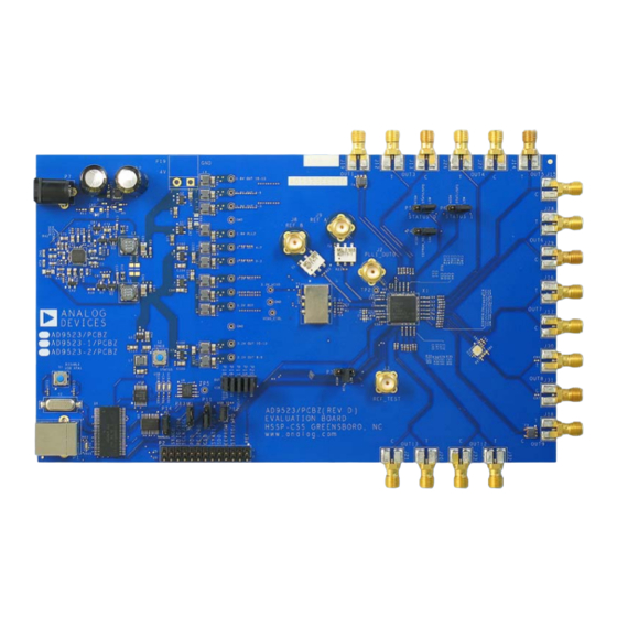
DIGITAL PICTURE OF EVALUATION BOARD
Figure 1.
Evaluation Board User Guide
GENERAL DESCRIPTION
This user guide describes the hardware and software of the
AD9523
and
AD9524
schematics and PCB layout artwork. The AD9523 and AD9524
are designed to operate in the same manner. This user guide
serves both boards but refers to the AD9523.
The AD9523 is defined to support the clock requirements for
long-term evolution (LTE) and multicarrier GSM base station
designs. It relies on an external VCXO to provide the reference
jitter cleanup to achieve the restrictive phase noise requirements
necessary for acceptable data converter SNR performance.
The input receivers, oscillator, and zero delay receiver provide
both single-ended and differential operation. When connected
to a 30.72 MHz to 122.88 MHz reference clock and a VCXO of
either 30.72 MHz to 122.88 MHz, the device generates low
noise outputs from a range of 0.96 MHz to 983.04 MHz.
AD9523 Evaluation Board
Rev. 0 | Page 1 of 12
evaluation boards, and includes detailed
UG-169
Advertisement
Table of Contents

Related Manuals for Analog Devices AD9523


Summary of Contents for Analog Devices AD9523
-
Page 1: Features
SMA connectors for serves both boards but refers to the AD9523. 2 reference inputs The AD9523 is defined to support the clock requirements for 2 PLL status outputs long-term evolution (LTE) and multicarrier GSM base station 1 reference test input designs. -
Page 2: Table Of Contents
EEPROM Control ..............11 Using I C Serial Port Mode ............4 Quick Start Guide to the AD9523 ..........12 Evaluation Board Software Setup ........... 5 Installing the Software ..............5 REVISION HISTORY 7/10—Revision 0: Initial Version... -
Page 3: Evaluation Board Hardware
Set up the power and PC connections as follows: the dc-to-dc converter only. This is useful for measuring the AD9523 power consumption. Refer to the evaluation board Install the AD9523 evaluation software before connecting schematics provided on the CD in the evaluation board kit (also the evaluation board to the PC for the first time (see the available at www.analog.com) for further details. -
Page 4: Using I C Serial Port Mode
UG-169 Evaluation Board User Guide USING I C SERIAL PORT MODE Select the desired I C address using Jumpers P5 and P6 (see Figure 3). Note that setting P5 and P6 low is reserved for SPI mode. On the evaluation software, select Configure Serial Port from the I/O menu (see the I/O Menu section). -
Page 5: Evaluation Board Software Setup
To install the software, the software runs in standalone mode. Standalone mode is Insert the AD9523 evaluation software CD-ROM into a PC useful for viewing and generating register setup files. CD disc drive. -
Page 6: Software Operation
WRITE button on the main window may start blinking. This blocks of the AD9523 (see Figure 6). These subsections, most of indicates that there are settings that have not been loaded to the which have their own window, are outlined in this section. -
Page 7: Menu Bar Of Main Window
File Menu The File menu allows you to load a previously saved AD9523 setup file or to save a new AD9523 setup file. A setup file (.stp) is a text file that contains the AD9523 register setup file, plus any evaluation board settings. -
Page 8: Using The Software To Control The Functional Blocks Of Ad9523
(see Help Menu Figure 13 for an example for the REF A Divider window). Selecting Help from the Help menu opens the About AD9523 window, which contains information such as revision number, region information, and contact information. -
Page 9: Pll 2 Controls
Evaluation Board User Guide UG-169 Feedback (N) Divider Window Figure 14. N Divider Window The feedback divider window shown in Figure 4 is accessed by clicking the N DIVI DER box in Figure 12. It a llows you to set the feedback divider. -
Page 10: Channel Divider Window
Figure 6. It is usually sufficient to change only the divide ratio, because the evaluation software and the AD9523 duty cycle correction feature ensure that the output duty cycle remains very close to 50%. Figure 24. Output Drivers It is important to power down unused outputs on the evaluation board, because they can be a major source of unwanted spurs. -
Page 11: Eeprom Control
EEPROM button near the lower left corner of the main window. To store the current register settings of the AD9523 to the EEPROM, click the Program EEPROM button. Visually confirm the EEPROM Status Registers section on the right side of the window to verify that the operation is successful. -
Page 12: Quick Start Guide To The Ad9523
By using the evaluation board discussed herein (together with any tools, components documentation or support materials, the “Evaluation Board”), you are agreeing to be bound by the terms and conditions set forth below (“Agreement”) unless you have purchased the Evaluation Board, in which case the Analog Devices Standard Terms and Conditions of Sale shall govern. Do not use the Evaluation Board until you have read and agreed to the Agreement.
Need help?
Do you have a question about the AD9523 and is the answer not in the manual?
Questions and answers