Table of Contents
Advertisement
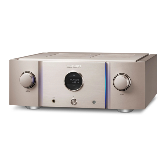
Integrated Amplifier
PM-10
• For purposes of improvement, specifications and design are subject to change without notice.
• Please use this service manual with referring to the operating instructions without fail.
• Some illustrations using in this service manual are slightly different from the actual set.
Service Manual
Click here!
On-line service parts list
http://dmedia.dmglobal.com/Document/DocumentDetails/23029
(P5 to P7)
Online Parts List
On-line owner's manual
http://manuals.marantz.com/PM10/NA/EN/index.php
http://manuals.marantz.com/PM10/EU/EN/index.php
http://manuals.marantz.com/PM10/AP/ZH/index.php
CAUTION IN SERVICING
ELECTRICAL
MECHANICAL
REPAIR INFORMATION
UPDATING
Please refer to the MODIFICATION NOTICE.
Ver. 3
Advertisement
Table of Contents

Related Manuals for Marantz PM-10


Summary of Contents for Marantz PM-10
- Page 1 Service Manual Ver. 3 Integrated Amplifier Click here! PM-10 On-line service parts list http://dmedia.dmglobal.com/Document/DocumentDetails/23029 (P5 to P7) Online Parts List On-line owner’s manual http://manuals.marantz.com/PM10/NA/EN/index.php http://manuals.marantz.com/PM10/EU/EN/index.php http://manuals.marantz.com/PM10/AP/ZH/index.php CAUTION IN SERVICING ELECTRICAL MECHANICAL REPAIR INFORMATION UPDATING • For purposes of improvement, specifications and design are subject to change without notice. Please refer to the MODIFICATION NOTICE.
-
Page 2: Caution In Servicing
CAUTION IN SERVICING SAFETY PRECAUTIONS NOTE FOR SCHEMATIC DIAGRAM NOTE FOR PARTS LIST INSTRUCTIONS FOR HANDLING SEMICONDUCTORS AND OPTICAL UNIT Online Parts List Accessing the Parts List Logging in to New SDI and Accessing the Parts List Accessing the Part List from the Model Asset Screen PRINTED CIRCUIT BOARDS Parts Table Downloading the Parts List as an Excel File Revision History... -
Page 3: Safety Precautions
SAFETY PRECAUTIONS ◎ Make a safety check after servicing! The following items should be checked for continued protection of the customer and the service Check that all screws, parts and wires removed or disconnected when servicing have been put back technician. -
Page 4: Note For Schematic Diagram
NOTE FOR SCHEMATIC DIAGRAM WARNING: Parts indicated by the z mark have critical characteristics. Use ONLY replacement parts recommended by the manufacturer. CAUTION: Before returning the set to the customer, be sure to carry out either (1) a leakage current check or (2) a line to chassis resistance check. - Page 5 Online Parts List Accessing the Parts List Logging in to New SDI and Accessing the Parts List (1) Click the URL link on the cover of the service manual. (1) Access New SDI from the URL below. Examples of display <http://dmedia.dmglobal.com>...
-
Page 6: Revision History
Accessing the Part List from the Model Asset Screen Downloading the Parts List as an Excel File (1) Display Model Asset from New SDI. (1) Displays the Parts List. Click the Download icon. (2) Click the section displayed as ▼ Link to Part Lists under the model name. NOTE : If the ▼... - Page 7 Searching Part Numbers or Ref. Numbers You can search a Parts List for part numbers or Ref. numbers. (1) Enter the part number or Ref. number in the search window of the Parts List, and press the search button. (2) The search results are displayed. The name of the sheet in which the search part is used and the part’s line are displayed.
-
Page 8: Initializing This Unit
CAUTION IN SERVICING. Initializing This Unit Make sure to initialize this unit after replacing the microcomputer or any peripheral equipment, or the PCB. 1. Press the power button to turn off the power. 2. Turn on the power. When the ID appears in the display, press and hold button "F.C.B.S. ID" for 5 seconds or longer. -
Page 9: Schematic Diagrams
ELECTRICAL SCHEMATIC DIAGRAMS LEVEL DIAGRAM SCH01_PHONO_HP_BACKLIGHT_P.SW SCH02_UCOM_LED L R_VOLUME BLOCK DIAGRAM SCH03_POWER_INDCTOR SCH04_XLR IN_VOLUME AMP 1 POWER DIAGRAM SCH05_XLR IN_VOLUME AMP 2 SCH06_XLR IN_VOLUME AMP 3 SCH07_FCBS WIRING DIAGRAM SCH08_RCA IN PWB 1 SCH09_RCA IN PWB 2 SCH10_RCA IN PWB 3 SEMICONDUCTORS SCH11_AC SCH12_CONNECT... - Page 10 SCHEMATIC DIAGRAMS SCH01_PHONO_HP_BACKLIGHT_P.SW R4079 D4018 D4019 R4001 F,U: 10 N,K: 33 R4015 R4061 N4001 R4003 D4101 D4103 R4095 R4097 N4004 +VCC 1SS133 1SS133 F,U: 39 2P-EH N,K: 100 C4007 +OUT L4001 L4003 47/25 R4009 3 +I N R4053 PHONO L ch -I N R4101 150uH...
- Page 11 SCH02_UCOM_LED L R_VOLUME Q1027 +3.3VL KRA102S C1064 +15V +3.3VD 0.1Z 8U-210216-5 C1002 C1065 POWER 1000P 0.22 +3.3VL C1003 No Si g nal : L BLUE LED L UNIT C1066 N1015 N1015 6P-PH 1000P Si g nal Det e ct : H KRC102S L1002 D-GND...
- Page 12 SCH03_POWER_INDCTOR N8103 N8103 11P-EH 8U-210216-2 +5VA +20V POWER PWB -20V -18V TO N4508 +18V A-GND +15V. PROTECT2 -15V. R8112 +24V L-GND Z8107 N8100 TR_SHI L ED From Mai n Trans 44541021300AS Z8106 3P-VH Z8102 SCREW D-GND. N8100 N8101 2SC4883(O/Y) D8101 HEAT_SINK_W36.2xL50 00M51100308M9 N8101...
- Page 13 SCH04_XLR IN_VOLUME AMP 1 N4505 N4505 4P-EH(I M ) 1 UNBAL_R+ 2 UNBAL_R- +21.3V +19.8V 3 UNBAL_L+ 4 UNBAL_L- +20V TO N3002 R4533 N4501 SHORT +24V +VCC R4534 R4521 +OUT SHORT C4529 -20V 3 +I N VI _ L- K4501 C4513 -I N R4517...
- Page 14 SCH05_XLR IN_VOLUME AMP 2 R5005 C5041 C5025 Z5002 470/16 R5065 Z5004 VO_L- OPEN M3_TOP 22/25 OPEN +15V Point B TO 1A +5.0V Point D R5089 Point A A-GND R5101 C5069 +VCC +VCC 2P-EH N5014 +OUT +OUT C5026 3 +I N R5025 3 +I N VI _ L+...
- Page 15 SCH06_XLR IN_VOLUME AMP 3 R9937 +18V +24V R9913 U9901 NJM2114M C9901 R9905 R9915 C9913 22/25 1.8K R9917 47/25 R9919 A-GND N9901 C9902 R9906 N9901 +24V 22/25 1.8K A-GND 5P-EH(I M ) HP_DET 1 HP_DET -18V R9939 2 D_GND 3 HP_L HP_RELAY 4 A_GND HP on:3.3V...
- Page 16 SCH07_FCBS K1901 RCA-PI N -JACK-2P 7P-FFCs N1902 1 TOOL0 2 RESET 3 NC 4 D_GND 5 +VCC C1901 6 RXD 0.1Z R1909 7 TXD R1908 OPEN Z1901 C1913 KRA104S M3-SIDE Q1902 Q1904 OPEN 0.1Z S1901 KRC102S JSS2208A N1904 Q1903 N1904 KRC104S K1902 3P-PH...
- Page 17 SCH08_RCA IN PWB 1 8U-210217-2 RCA IN PWB 1/3 (STY-PIN) Z2001 OPEN +24V. N2001 9P-EH N2001 +20V. UNBAL_L +20V -20V. -20V PHONO_L TO 2A A-GND A-GND to RCA IN PWB 3/3 PHONO_R +24V. +24V A-GND. +3.3V: MM functi o n UNBAL_R MC_HIGH 0V: MC-hi g h/Low functi o n...
- Page 18 SCH09_RCA IN PWB 2 8U-210217-2 RCA IN PWB 2/3 +24V. POWER AMP DI R ECT I N K3602 P_DI _ L to RCA IN PWB 1/3 +18V. U3902 6 8 4 R3904 NJM2068MD RO_L. TO A6 A-GND. D3907 from RCA IN PWB 1/3 R3905 RO_R.
- Page 19 SCH10_RCA IN PWB 3 8U-210217-2 R3077 SHORT +20V. RCA IN PWB 3/3 R3083 N3021 N3023 R3083-R3086 +VCC +VCC R3041/42/75/76 はor使い +OUT +OUT C3027 R3041 3 +I N 3 +I N -I N -I N 100/25 OPEN -OUT -OUT -VCC -VCC -20V.
- Page 20 SCH11_AC N8502 N8503 TO N8803 TO N8901 To Power SW PWB To INDUCTOR PWB N8901 N8803 2P-VHw N8502 N8503 2P-VHw N8504 TO N8100 Measurement condition To Power PWB C8505 N8100 ・ Voltage measurement 0.01 No signal TO N8501 S8501 To Standby PWB RELAY_DLS1U N8501 ・...
- Page 21 SCH12_CONNECT NC500 L+ NC500 L- NC500 R- NC500 R+ Z6010 Z6011 MA001 MA002 MA003 MA004 Z6014 Z6013 GND1 GND1 GND1 GND1 Z6001 GND1 GND1 GND1 GND1 +62.0V STYLE-PIN Z6002 STYLE-PIN GND1 GND1 GND1 GND1 -15.4V CLIP (NC500 Cl i p i n di c ati o n) Q6003 Q6006 Q7003...
- Page 22 SCH13_SEL SW 8U-310221-5 SEL SW UNIT R1271 R1268 R1266 R1265 R1264 R1263 R1262 R1261 R1260 R1259 R1258 R1257 R1256 R1255 R1254 R1253 R1251 2.2K 2.2K 120K 1.8K 1.2K 1.5K 1.5K 1.5K 3.9K 1.5K 4.7K R1269 R1252 R1267 1.8K 2.2K 120K B1251 B1251 4P-EH-SCN...
- Page 23 SCH14_SPK From UCOM PWB N9505 N1004 TO N1004 Z9502 Z9503 STYLE-PIN STYLE-PIN N9504 3.3V N9504 12P-PH C9523 IOUT_L. +HV_L. I O UT_L. 1 IOUT_L OPEN I O UT_R. -HV_L. 2 IOUT_R 3.3V 3 AMPON 3.3V 4 CLIP 5 READY 6 SCCPIND 7 FATAL R9551 +HV_L.
- Page 24 SCH15_REG 8U-310221-4 REG PWB 2SC4883(O/Y) Q5801 R6037 +VSI G _L. +15V_L. UDZS8.2B UDZS7.5B UDZS7.5B GND1. UDZS8.2B N6008 9P-EH OPEN N6008 Z6016 +VSI G _L. R6038 -VSI G _L. -VSI G _L. -15V_L. -15V_L. Q5802 2SA1859(O/Y) +15V_L. TO N6007 2SC4883(O/Y) +15V_R. Q5901 R6039 -15V_R.
- Page 25 PRINTED CIRCUIT BOARDS UCOM, POWER SW, BACKLIGHT, LED L, LED R, VOLUME, HP, INDUCTOR, POWER, PHONO Lead-free Solder When soldering, use the Lead-free Solder (Sn-Ag-Cu). UCOM (A SIDE) UCOM (B SIDE) POWER (A SIDE) POWER (B SIDE) BLUE N1001 N1015 N1007 8U-210216-3 N1005...
- Page 26 AUDIO IN, RCA, FCBS, SPACER AUDIO IN (A SIDE) AUDIO IN (B SIDE) RCA (A SIDE) RCA (B SIDE) SPACER (A SIDE) FCBS (A SIDE) FCBS (B SIDE)
- Page 27 SPK, AC, REG, SEL SW, CONNECT SPK (A SIDE) SPK (B SIDE) AC (A SIDE) AC (B SIDE) REG (A SIDE) REG (B SIDE) C6038 C6039 8U-310221-3 C6040 SPK UNIT C6037 Z9504 N9506 D8505 Z6016 D8502 D8525 D8526 R9503 C8501 L8501 D8523 D8504...
-
Page 28: Level Diagram
LEVEL DIAGRAM Volume Setting PM-10S1 LEVEL DIAGRAM 0dB (MAX) +40dB SPK OUT 40V (8ohms, 200W) +30dB +6.0dB +20dB +18.4dB +10dB -1.5dB P.AMP IN +6.0dB CD,LINE,REC : +9.5dB P.DIRECT IN 1.5V BALANCED,PHONO:+15.5dB CD,LINE,PHONO : -6.0dB +6.0dB(CD, LINE, REC) CD, LINE, REC 440mV BALANCED: 0dB REC OUT 440mV BALANCE 880mV... -
Page 29: Block Diagram
BLOCK DIAGRAM PM-10S1 BLOCK DIAGRAM PHONO EQUALIZER PHONO SPEAKER NC500 RIAA RIAA SPK A CLASS D OUTPUT STAGE NC500 SPK B LINE1 HP AMP HEADPHONE LINE2 HP DETECT POWER BAL1 LINEAR CONTROL VOLUME Darlington Push-Pull BAL2 HDAM-SA3 HDAM-SA3 module (on board) REC OUT BUFFER Darlington Push-Pull... -
Page 30: Power Diagram
POWER DIAGRAM... -
Page 31: Wiring Diagram
WIRING DIAGRAM... - Page 32 SEMICONDUCTORS Only major semiconductors are shown, general semiconductors etc. are omitted to list. The semiconductor which described a detailed drawing in a schematic diagram are omitted to list. 1. IC's R5F100MFAFA (U1004) PORT TABLE Port Setting Port I/O use Name Note Act.
- Page 33 Port Setting Port Setting Port I/O use Name Note Port I/O use Name Note Act. stby Exit R Act. stby Exit R P74/KR4/INTP8 VOL_A PU 10k Volume Rotary Encorder LCD Driver Communication mode setting input P22/ANI2 D_SET PD 47k H/L = Communication during communication / opera- P73/KR3 tion at 100 msec P72/KR2/SO21...
- Page 34 CD4094BPWR (U2501, U2502) U2501 Port Setting PIN ASSIGNMENT Port I/O use Name Note Act. stby Exit R STROBE STROBE Chip Enable OUTPUT DATA ENABLE DATA DATA Serial Data (Direct controll from MPU) CLOCK CLOCK Serial Clock LINE2 PD 10k LINE2 INPUT Relay ON (ON:H) PD 10k RECORDER INPUT Relay ON (ON:H) BAL2...
- Page 35 TC74VHC86FT (U1003) MAS6116 (U5001, U5002) SO16 AVCC AGND ROUT LGND RGND RGND DGND PEAK ZERO DVCC CCLK CROSSING DETECTOR DATA XMUTE DATA CCLK CONTROL XMUTE ZERO PEAK CROSSING DETECTOR LOUT LGND AGND MAS6116 AVCC DVCC DGND Pin Name Type Function SO16 QFN 4x5 AVCC...
- Page 36 74VHCT14AFT (U5003) 2. DISPLAY PIN ASSIGNMENT IEC LOGIC SYMBOL LCD (DP-0010) (VD01) 1Pin 11Pin Display Side PIN CONNECTION TRUTH TABLE Symbol Function Liquid crystalline drive bias input pin Liquid crystalline drive bias input pin Liquid crystalline drive bias input pin Power supply for the liquid crystalline drive Logic power supply Power supply (0 V...
- Page 37 MECHANICAL DISASSEMBLY Flowchart 1. AUDIO IN PCB 2. SMPS ASSY 3. FRONT PANEL ASSY 4. RCA PCB 5. POWER PCB 6. PHONO ASSY 7. INDUCTOR PCB 8. AC PCB 9. POWER TRANS 10. AMP ASSY 11. REAR PANEL ASSY EXPLODED VIEW PACKING VIEW...
- Page 38 DISASSEMBLY Flowchart • Remove each part following the flow below. • Reassemble the removed parts in the reverse order. • Read "SAFETY PRECAUTIONS" before reassembling the removed parts. • If wire bundles are removed or moved during adjustment or part replacement, reshape the wires after completing the work. Failure to shape the wires correctly may cause problems such as noise. •...
- Page 39 Explanatory Photos for DISASSEMBLY 1. AUDIO IN PCB • For the shooting direction of each photos used in this manual, see the photo below. • A, B, C and D in the photo below indicate the shooting directions of photos. Proceeding : TOP COVER →...
-
Page 40: Front Panel Assy
2. SMPS ASSY 3. FRONT PANEL ASSY Proceeding : TOP COVER → SIDE PANEL → SMPS ASSY Proceeding : TOP COVER → SIDE PANEL → AUDIO IN PCB → SMPS ASSY (1) Remove the screws. → FRONT PANEL ASSY (1) Remove the screws. View from the bottom (2) Remove the screws. - Page 41 4. RCA PCB 6. PHONO ASSY Proceeding : TOP COVER → SIDE PANEL → AUDIO IN PCB → RCA PCB Proceeding : TOP COVER → SIDE PANEL → AUDIO IN PCB → RCA PCB → PHONO ASSY (1) Remove the screws. Remove the connector. Remove the STYLE PIN. (1) Remove the screws.
-
Page 42: Power Trans
8. AC PCB 10. AMP ASSY Proceeding : TOP COVER → SIDE PANEL → INDUCTOR PCB → AC PCB Proceeding : TOP COVER → POWER TRANS → AMP ASSY (1) Remove the screws. Remove the connector. (1) Remove the screws. Remove the connector. Remove the STYLE PIN. from POWER PCB B8102 AMP Lch RED N9504... -
Page 43: Exploded View
EXPLODED VIEW Parts List 001L http://dmedia.dmglobal.com/Document/DocumentDetails/23029 817G 085G 823G 003L 817G 074G 085G 803G 813G MA001 MA002 MA003 MA004 068G 085G 817G 075G 003L 068G 073G 085G P3-1 067G 815G 807G 012D 001D 006D 053G 807G 815G MP002 901G 810G 001L 023G J001... -
Page 44: Packing View
PACKING VIEW Parts List For N : 001T 002T 003T 007T http://dmedia.dmglobal.com/Document/DocumentDetails/23029 For U : 001T 003T 008T 009T 007T For F : 001T 003T 006T 007T UK plug For K : 001T 003T 007T 011S 010S (UK Only) W001 009S 010S B0001... -
Page 45: Repair Information
REPAIR INFORMATION TROUBLE SHOOTING 1. The power cannot be turned on (STANDBY LED is not lit(STANDBY MODE)) 2. The power cannot be turned on (STANDBY LED is lit→light flashes) 3. STANDBY LED flashes while using the unit (Protection circuit becomes activated) 4. -
Page 46: The Power Cannot Be Turned On
TROUBLE SHOOTING 1. The power cannot be turned on 2. The power cannot be turned on (STANDBY LED is not lit(STANDBY MODE)) (STANDBY LED is lit → light flashes) INDUCTOR PCB Check insertion of each connector. Check insertion of the connector. AC PCB When the power is turned on, does the LCD light Check insertion of the connector. - Page 47 3. STANDBY LED flashes while using the unit (Protection circuit becomes activated) "2. The power cannot be turned on (STAND- Check insertion of each connector. BY LED is lit → light flashes)" 4. The power turns on but no sound is output 4.1.
-
Page 48: Measuring Method And Waveforms
MEASURING METHOD AND WAVEFORMS It is recommended to use extension wires between the probe and test points. AUDIO IN PCB : U5001, U5002 [MAS6116] RCA IN PCB : U2501, U2502 [CD4094BPWR] 1. PCB test point • For points q to Q1 , take measurements at the points shown in the diagram below. r 1pin AUDIO IN PCB : U5001, U5002 [MAS6116] STROBE... - Page 49 ADJUSTMENT Adjusting Idling Current Set the power voltage to the rated voltage for this adjustment. 1. Preparation DC Voltmeter (1) Prepare a DC voltmeter. (2) Place the unit under normal usage conditions, away from highly ventilated areas such as next to an air conditioning machine or electric fan.
-
Page 50: Special Mode Setting Button
SPECIAL MODE Special mode setting button b No. 1 : Turn on the power. When the ID appears in the display, press and hold button "A" for 5 seconds or longer. Mode Button A Button B Descriptions The firmware version, display check, communication test of BUS, protection detection count and serial number display appear in the display. Service mode F.C.B.S. -
Page 51: Service Mode
1. Service mode 1.4. Initialization item 1.1. Actions The firmware version, display check, communication test of BUS, protection detection count and serial Items Default number display appear in the display. INPUT SELECTOR The memory is cleared and the unit is initialized. VOLUME - ∞... - Page 52 2. ERROR MESSAGES Displayed when an error occurs. No. Error cord Error content Remedies ID=1(Master) Two or more amplifiers set as ID=2 (Slave) were detected. Two or more amplifiers set as ID=3 (Slave) were detected. Assign different ID numbers to the amplifiers. Two or more amplifiers set as ID=4 (Slave) were detected.
-
Page 53: Protection Operation
3. Protection operation Explanation of UCOM (U1004) [PROT_1 : pin1, PROT_2 : pin2, PROT_4 : FATAL, pin31, PROT_5 : READY, pin40, PROT_6 : M_B_DOWN, pin75] [B] The PROT_2 (pin2) is the port to detect abnormalities of the power [A] The PROT_1(pin1) is the port to detect the following abnormalities of supply circuit the Power Amplifiers (1) Detection of an abnormality in the DC offset voltage from the Speaker Output terminal. - Page 54 [C] PROT_4(FATAL,pin31) is the port for detecting a power amplifier ab- [D] PROT_5(READY,pin40) is the port for detecting abnormalities in the normality or SMPS abnormality SMPS and power amplifier (1) Detection of an abnormality in the DC offset voltage from the Speaker Output terminal. (1) Detection of an abnormality in the power amplifiers power supply circuit ( ±...
- Page 55 [E] The PROT_6(M_B_DOWN, pin75) is the port to detect abnormalities of the power supply circuit PM-10S1 Protection Chart (Possible Factors) · SHORT of ±20V type +24V overcurrent detection for Relay (Detection of a current of 133mA or (1) Detection of an abnormality in the LED power supply circuit. higher passing through +24V) When an undervoltage (around 11.3V) is detected in +15V of the LED power supply, [Q1004, Q1006] (Possible Factors)
- Page 56 UPDATING PROCEDURE AFTER REPLACING THE PCB. PROCEDURE AFTER REPLACING THE U-COM, ETC.
- Page 57 PROCEDURE AFTER REPLACING THE PCB. PROCEDURE AFTER REPLACING THE U-COM, ETC. The procedure after replacing the printed circuit boards is as follows. The procedure after replacing the u-COM (microprocessor), flash ROM, etc. is as follows. (1) Change the resistor for setting the region. Procedure PCB Name Ref.
- Page 58 Copyright © 2017 D&M Holdings Inc. All Rights Reserved.
Need help?
Do you have a question about the PM-10 and is the answer not in the manual?
Questions and answers