Table of Contents
Advertisement
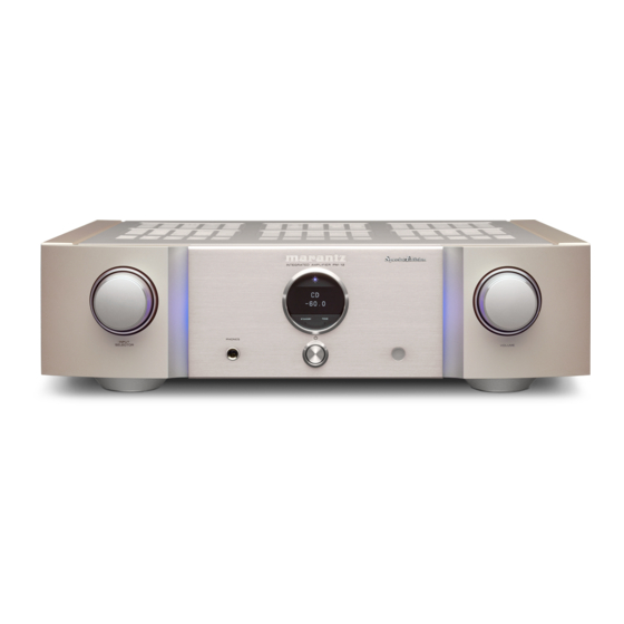
PRE-MAIN AMPLIFIER
PM-12 SE
PM-12 OSE
• For purposes of improvement, specifications and design are subject to change without notice.
• Please use this service manual when referring to the operating instructions without fail.
• Some illustrations used in this service manual are slightly different from the actual product.
Service Manual
Click here!
On-line service parts list
PM-12 SE:
https://dmedia.soundunited.com/documents/details/26617
PM-12 OSE:
https://dmedia.soundunited.com/documents/details/26616
ONLINE PARTS LIST
(P5)
WEB owner's manual
EU:
http://manuals.marantz.com/PM12SE/EU/EN/index.php
JP:
http://manuals.marantz.com/PM12OSE/JP/JA/index.php
Upload is planned for the time of a future press release.
BEFORE SERVICING THIS UNIT
ELECTRICAL
MECHANICAL
REPAIR INFORMATION
UPDATING
Confidential
Ver. 1
Advertisement
Table of Contents


Need help?
Do you have a question about the PM-12 SE and is the answer not in the manual?
Questions and answers