
Subscribe to Our Youtube Channel
Related Manuals for NXP Semiconductors OM13260


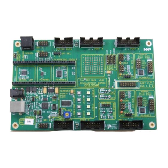
Summary of Contents for NXP Semiconductors OM13260
- Page 1 Installation Guide Installation Guide for OM13320 Preliminary 1 — 9/6/2013 Installation Guide Document information Info Content Keywords Abstract Installation Guide for the Fm+ Development Board (OM13260) Kit...
-
Page 2: Contact Information
NXP Semiconductors Revision history Date Description Preliminary 1 Sept . 5, 2013 First Draft of document Contact information For more information, please visit: http://www.nxp.com For sales office addresses, please send an email to: salesaddresses@nxp.com UMxxxxx All information provided in this document is subject to legal disclaimers. -
Page 3: Key Features
NXP Semiconductors Install Guide for OM13320 1. Introduction The Fm+ Development Kit (OM13320) is intended for several different tasks; from a hands-on introduction, understanding, and use of the I2C (Inter-Integrated Circuit) Bus, to I2C device evaluation, and as a simple product demonstration platform (for trade shows and sales pitches). -
Page 4: Kit Contents
FM+DevelopmentBoard V03_00.bin 19kb Standalone_trade_show_FM+_DEMO.bin The “Trade Show” mode activates the LEDs on the Fm+ Development Board (OM13260) and also on the optional GPIO Target Boards (OM13303) if attached. This “Blinky lights” are a suitable demonstration for Trade Shows. Kit Contents Before using the kit for the first time, please familiarize yourself with the various components, as shown in Table 3.1 See figure 3.1 and figure 3.2... -
Page 5: Box Contents
These should be retained in the box for future access. Depending upon the desired use some of the PCB assemblies may be attached to each other, either by plug connection or by ‘stacking’ the GPIO PCB assemblies above the Fm+ Development Board (OM13260), using the supplied ribbon cables and hardware. - Page 6 Bus Buffers bridge two I2C Bus segments, which are provided on the Fm+ Development Board (OM13260) by Bus1 and Bus2. Bus Buffer Daughter Cards, such as the PCA9617A Bus Buffer Demo Board (OM13398) (Supplied in the kit) can be installed directly on Port E (CN12). See figure 3.5 UMxxxxx All information provided in this document is subject to legal disclaimers.
- Page 7 NXP Semiconductors Fig 3.5 OM13260 Bus Buffer PCB Assembly 3.3.4 Bridge Board (OM13398) Some existing Demo Boards used a single row connector with nine pins. To use these with the Fm+ Development Kit requires the Bridge Board (OM13399, supplied in the kit). See figure 3.6 Fig 3.6 OM13399 Bridge Board PCB Assembly...
- Page 8 If a dedicated Daughter Card is not available for a specific new device, it can still be added to the Fm+ Development Board (OM13260) using the EVM (Evaluation Module) (OM13490). See figure 3.8 and figure 3.9. Sample devices are attached using DIP Adapter Boards, which in turn are plugged into the EVM Board.
- Page 9 NXP GUI Firmware. First time set up of the Fm+ Development Board (OM13260) Several jumpers must be installed before using the Fm+ Development Board (OM13260) PCB. The on board microcontroller (MCU) must contain the appropriate firmware. There are two distinct applications (“Trade Show”...
- Page 10 NXP Semiconductors Table 4.1 OM13260 Jumpers Jumper Label Function First Time XPRESSO Close POWER Open CONNECT Close Open PCA9955 Address Open SPI SEL JP10 PCA9672 Address JP11 SDA1 Pull Up JP12 SCL1 Pull Up JP13 Bus1 Bus Voltage JP20 PCA9672...
- Page 11 4.4. OM13260 Port E By-pass Depending up the intended operation of the Fm+ Development Board (OM13260), Port “E” (CN12) should be left open, or linked with a jumper wire, or for the attachment of a Bus Buffer Board. The PCA9617A Bus Buffer Demo Board (OM13398) is supplied in the kit.
- Page 12 Figure 4.4. The following four steps must be completed: 1. Attach the completed Fm+ Development Board (OM13260) to the computer via USB cable (supplied in the kit) 2. Using the Device Manager, remove the default USB driver 3.
- Page 13 NXP Semiconductors Fig 4.5 Windows Device Manager Fig 4.6 Windows Device Manager UMxxxxx All information provided in this document is subject to legal disclaimers. © NXP B.V. 2013. All rights reserved. Preliminary 1 — September 6, 2013 Install Guide 13 of 70...
- Page 14 NXP Semiconductors Fig 4.7 Windows dialog box Fig 4.8 Windows dialog box C:\Program Files (x86)\NXP FM+ Development Board Software\Drivers UMxxxxx All information provided in this document is subject to legal disclaimers. © NXP B.V. 2013. All rights reserved. Preliminary 1 — September 6, 2013...
- Page 15 NXP Semiconductors Fig 4.9 Windows dialog box Fig 4.10 Windows dialog box Fig 4.11 Windows Device Manager UMxxxxx All information provided in this document is subject to legal disclaimers. © NXP B.V. 2013. All rights reserved. Preliminary 1 — September 6, 2013...
- Page 16 4.7.1 “Trade Show” Mode A popular use of the Fm+ Development Board (OM13260) kit is for publicity and promotion of the I2C Bus products from NXP. A version of the firmware provides “Blinky Lights” on the Fm+ Development Board (OM13260) PCB, and the optional attached GPIO Target Boards OM13303.
- Page 17 Development Board (OM13260) is connected. Note: To restore operation as a “Trade Show” demo, the firmware on the Fm+ Development Board (OM13260) must be reset to “Trade Show” mode by installing the correct firmware. (See section 4.8). OM13260 Firmware Installation Access to the on board MCU firmware is made through the USB port (CN5).
- Page 18 NXP Semiconductors Fig 4.13 Fm+ Development Board MCU factory supplied firmware (Win7 OS) Fig 4.14 Fm+ Development Board MCU project specific firmware (Win7 OS) UMxxxxx All information provided in this document is subject to legal disclaimers. © NXP B.V. 2013. All rights reserved.
-
Page 19: Theory Of Operation
NXP Semiconductors 5. Fm+ Development Board (OM13260) The Fm+ Development Board (OM13260) PCB assembly is self-contained, requiring only DC power to operate. Depending upon the firmware installed on the Fm+ Development Board (OM13260) it can also operate with a connected Personal Computer (PC) via a USB cable. - Page 20 Power supplies and other signals are readily available. On the Fm+ Development Board (OM13260) V3.0 there is an LED Blinker device (PCA9901, IC3) and LED indicator (D10), while not strictly an I2C device, as it uses a one wire protocol, it belongs to the NXP I2C UMxxxxx All information provided in this document is subject to legal disclaimers.
-
Page 21: Circuit Description
5.2 and figure 5.3. Selection of the power source is automatic, using ORing diodes (D1 and D2). The main power on the Fm+ Development Board (OM13260) is 3.3V, from a linear regulator (IC1) but some of the circuits are powered directly from the incoming supply, which is a nominal 5V. Linear regulator (IC1) uses the PCB bottom layer copper as a heat sink. - Page 22 NXP Semiconductors Fig 5.2 Power Supply UMxxxxx All information provided in this document is subject to legal disclaimers. © NXP B.V. 2013. All rights reserved. Preliminary 1 — September 6, 2013 Install Guide 22 of 70...
-
Page 23: Usb Interface
NXP Semiconductors Fig 5.3 Power Supply and USB Section 5.2.2 USB Interface The USB Host connector (CN5) provides DC Power and USB connectivity using the MCU (IC5) hardware interface, see figure 5.3 and figure 5.4. USB data lines are terminated by resistors (R27 and R28) and protected by an ESD network (IC7). - Page 24 NXP Semiconductors Bus One (Bus1) There are two almost identical I2C Buses on the Fm+ Development Board (OM13260), called Bus1 and Bus2. These share a ground and power connection but may be operated independently. Note: The Bus Voltage for each I2C maybe different (for example 3.3V for one I2C bus, 5V for the other I2C bus).
- Page 25 Fig 5.6 MCU SWD Interface Section MCU Port0 and Port1 provide most of the signals used by the Fm+ Development Board (OM13260), see figures 5.7 and 5.8. I2C Bus1 is connected to the MCU Port0 via RC edge rate control networks that provide bus fall time control (SCL1;...
- Page 26 NXP Semiconductors Fig 5.8 IC5 MCU Port0 Fig 5.9 IC5 MCU Port1, Oscillator and Power Supply The HVQN32 package has a thermal pad ground connection, and operates from the main 3.3V supply. The MCU operates with a 12.00MHz crystal controlled oscillator, the frequency value and accuracy is necessary for correct USB timing, see figure 5.9.
- Page 27 NXP Semiconductors 5.3.2 Bus 1 Pull Up Resistors The Bus1 is pulled up to either the 3.3V or 5V supplies, via JP13. Three different value pull up resistors are provided by jumper selection, JP11 and JP12. The values of the pull up resistors are shown in table 5.1.
- Page 28 NXP Semiconductors Table 5.1 Bus Pull Up Resistors Strength Position Value Bus 1 SCL Bus 1 Bus 2 Bus 2 (Ohms) 1100 5.3.3 LED Driver Slave (PCA9955) Bus1 is also used to control the LED Driver (PCA9955, IC6). The LED Driver has constant current outputs and is directly connected to the LEDs, without customary series resistors.
- Page 29 NXP Semiconductors Fig 5.13 Bus1 LED Driver 16 channel Section Operation of all sixteen LEDs at maximum current will overheat the LED Driver, which is protected by an internal thermal limiter, the device will shutdown, and recover when the temperature has fallen.
- Page 30 NXP Semiconductors Table 5.1 LED Driver Address Selection HEX 8-bit NXP 7-bit 0xC0 1100 0000 0x60 0110 0000 0xD0 1101 0000 0x68 0110 1000 5.3.4 GPIO Slave (PCA9672) The GPIO (PCA9672, IC10) is connected to Bus1, and provides eight input/output channels at CN10.
- Page 31 Fig 5.15 Bus1 GPIO 8 bit Section Bus Two (Bus2) The second I2C Bus on the Fm+ Development Board (OM13260) requires the addition of a NXP LPC Xpresso Module (not included in the kit) to either be the Master, or drive the Bus Controller (PCA9665, IC4).
- Page 32 NXP Semiconductors I2C Bus2 is connected to the MCU Port0 via RC edge rate control networks that provide bus fall time control (SCL2; R45 and C23, SDA1; R44 and C19). See figure 5.18. Fig 5.16 Fm+ Development Board with LPC Xpresso installed Fig 5.17 LPC X presso Power (JP1)
- Page 33 NXP Semiconductors Fig 5.18 Bus2 Master (LPC Xpresso) 5.4.2 Bus 2 Bus Master (PCA9665) A second Bus Master is connected to Bus2 using a dedicated Bus Controller device (PCA9665 Fm+ parallel bus to I2C-bus controller) (IC4). The parallel port side is connected to the LPC Xpresso module (LPC1343 PIO2 and PIO3), the I2C side is connected via RC edge rate control networks that provide bus fall time control (SCL2;...
- Page 34 NXP Semiconductors Fig 5.19 Bus2 Master (PCA9665) Fig 5.20 Bus2 Master (PCA9665) Section 5.4.3 Bus 2 Pull Up Resistors The Bus2 is pulled up to either the 3.3V or 5V supplies, via JP23. Three different value pull up resistors are provided by jumper selection, JP21 and JP22. . The values of the pull up resistors are shown in table 5.2.
- Page 35 NXP Semiconductors Fig 5.21 Bus2 Pull Ups and Bus Voltage Selector Fig 5.22 Bus2 Pull Ups Section UMxxxxx All information provided in this document is subject to legal disclaimers. © NXP B.V. 2013. All rights reserved. Preliminary 1 — September 6, 2013...
- Page 36 NXP Semiconductors Table 5.2 Bus Pull Up Resistors Strength Position Value (Ohms) 1100 UMxxxxx All information provided in this document is subject to legal disclaimers. © NXP B.V. 2013. All rights reserved. Preliminary 1 — September 6, 2013 Install Guide...
-
Page 37: Daughter Card Ports
The PCA9617A Bus Buffer Demo Board (OM13398) (Supplied in the kit) is an example. The Fm+ Development Board (OM13260) may also be operated with nothing connected to Port E (CN12). The Port E signal pins are arranged to be symmetrical, permitting the card to be rotated 180degress, effectively changing the direction of the signals through the card. - Page 38 NXP Semiconductors linked together by wire jumper the pull-up resistors on each Bus are effectively in parallel. The resulting value is therefore one half of the original value. Pull-up resistors of low value will overload the I2C drivers, and effectively stop the bus from operating.
- Page 39 NXP Semiconductors Fig 5.27. Bus1 and Bus2 Tester connectors Fig 5.28. Bus1 Tester connectors Fig 5.29. Bus2 Tester connectors UMxxxxx All information provided in this document is subject to legal disclaimers. © NXP B.V. 2013. All rights reserved. Preliminary 1 — September 6, 2013...
-
Page 40: Serial Communication Port
NXP Semiconductors Serial Communication Port The LCP Xpresso module has a serial comms (communications) port, EIA232 standards compliant using IC2, a voltage level translator. See figure 5.30. This is provided for connection to I2C Bridge devices that require Serial Communications. - Page 41 NXP Semiconductors Fig 5.32 Serial Com Section SPI Ports Both the Bus1 Master MCU and the Bus2 Master LPC Xpresso Module support SPI communications. The Bus1 MCU has one SPI port (SPI2) (CN16) and the LPC Xpresso has two SPI ports (SPI0 and SPI1)(CN9 and CN8 respectively).
- Page 42 NXP Semiconductors Fig 5.34. SPI 2 (Bus1 MCU) connector Fig 5.35. SPI 0 and SPI 1 (Bus2 LPC Xpresso) connectors 5.10 Logic Probe Most of the I2C Slaves produce logic signals, on their Input-Output ports. It is necessary to know a logic state.
- Page 43 NXP Semiconductors Fig 5.36. Logic Probe circuit Fig 5.37. Logic Probe section (shown monitoring two GPIO channels from Bus1) UMxxxxx All information provided in this document is subject to legal disclaimers. © NXP B.V. 2013. All rights reserved. Preliminary 1 — September 6, 2013...
- Page 44 5.39. Additional buffered LEDs are provided (D19, RST and D20, Interrupt) on the Fm+ Development Board (OM13260) for visual indication, these operate in the same fashion as the Logic Probe (see section 5.10 Logic Probe). Fig 5.38. INT and RST indicators circuit Fig 5.38.
-
Page 45: Prototype Area
Prototype Area Additional circuits may be required to for an application beyond the intended scope of the Fm+ Development Board (OM13260). For example, using different value pull-up resistors to those supplied, or other circuit experiments. The Prototype area is available, and consists of pads and holes on a 100mil (2.54mm) grid. Power for these components is made available at several connector points (CN15 is ground, CN21 is +3.3V, and CN22 is +5V). - Page 46 LED Blinker (PCA9901) On the Fm+ Development Board (OM13260) V3.0 there is an LED Blinker device (PCA9901, IC3) and LED indicator (D10), while not strictly an I2C device, as it uses a one wire protocol, it belongs to the NXP I2C Product portfolio.
-
Page 47: Theory Of Operation
GPIO Target Board is attached. A two by five header is used to connect to the Fm+ Development Board (OM13260) or a GPIO Daughter Card, with a flat ribbon cable (supplied in the kit). Two connectors are installed, one on each end of the board, and on opposite sides of the PCB to aid in connection without the cables blocking the buttons or LEDs. -
Page 48: Circuit Description
NXP Semiconductors Circuit Description The schematic diagram has multiple sheets. For clarification only fragments of the schematic are shown here. The full schematic should be downloaded if required. The following pages are divided in to several sections covering the Window Comparator, Push Switches, Bias Circuit, and Connectors. - Page 49 NXP Semiconductors Fig 6.3 Window Comparator (Channel0 shown) Fig 6.4 Input ramp (yellow trace), Green LED drive (green trace) UMxxxxx All information provided in this document is subject to legal disclaimers. © NXP B.V. 2013. All rights reserved. Preliminary 1 — September 6, 2013...
-
Page 50: Push Switches
NXP Semiconductors Fig 6.5 Input ramp (yellow trace), Red LED drive (green trace) 6.2.2 Push Switches Each channel has a push switch (S01 through S71) that connects the appropriate IO pin to ground when pressed. Series resistors (R01 through R71) limit the current, in the event that the IO pin is being driven high (by the connected GPIO device) when the push switch is closed. -
Page 51: Bias Circuit
NXP Semiconductors Fig 6.6 Push switches 6.2.3 Bias Circuit Each channel requires three reference voltages (VL, VC, and VH), from the Bias Circuit. A resistor divider chain (R01, R02, R03, and R04) divides the supply voltage to produce one-third (VL), one half (VC) and two-thirds (VH). - Page 52 The GPIO Target Board (OM13303) is intended to be connected to the Fm+ Development Board (OM13260) (or other GPIO Daughter Cards) via a ten pin ribbon cable. There are two identical connectors, one on each end of the GPIO Target Board to allow connection without blocking the push switches or the LEDs.
- Page 53 NXP Semiconductors Fig 6.8 Connectors Fig 6.9 Ribbon cables attached to the underside of the GPIO Target Board (OM13303) UMxxxxx All information provided in this document is subject to legal disclaimers. © NXP B.V. 2013. All rights reserved. Preliminary 1 — September 6, 2013...
- Page 54 NXP Semiconductors Fig 6.10 Ribbon cables attached to the topside of the GPIO Target Board (OM13303) UMxxxxx All information provided in this document is subject to legal disclaimers. © NXP B.V. 2013. All rights reserved. Preliminary 1 — September 6, 2013...
- Page 55 The Bus Buffer Board (OM13398) (supplied in the kit) provides a method to link both the I2C Busses on the Fm+ Development Board (OM13260) by attachment to Port E, in place of the wire jumper used earlier (see section 4.6.1 “Linking both Busses together (with a jumper)”. See figure 7.1 and figure 7.2.
- Page 56 Two identical Bus Buffer devices are connected in series between the Bus1 and Bus2 segments on the Fm+ Development Board (OM13260), each Bus Buffer has two identical channels, one for I2C Clock (SCL) and the second for I2C Data (SDA) only one channel will be described in detail.
- Page 57 Bus1 Bus Buffer (PCA9617A) I2C signals from the Fm+ Development Board (OM13260), called SCL1 and SDA1, are applied to the high voltage or ‘B’ Side of IC1 (PCA9617A). The required pull up resistors on this section of Bus1 are on the Fm+ Development Board (OM13260).
- Page 58 NXP Semiconductors Development Board (OM13260). The required pull up resistors on this section of Bus1 are on the Fm+ Development Board (OM13260). Fig 7.5 Bus2 Bus Buffer 7.2.3 Supply Select Jumpers The ‘B Side’ (high voltage side of the voltage level translator) of each PCA9617A can be either 3.3V or 5V as selected by JP1.
- Page 59 NXP Semiconductors Fig 7.6 Supply Select Jumpers 7.2.4 Variable Voltage Regulator The low voltage bus bias is generated by an LDO (Low Drop Out) voltage regulator, IC5. The output voltage is set by resistor divider R3, R4, and R5, and provides a range of 1.0V to 3.2V. The LDO provides a ‘Power Good’...
- Page 60 The connector on the Bus Buffer Board (OM13398) matches the Port E connector on the Fm+ Development Board (OM13260) See figure 7.7 and figure 7.8 The signals are arrange to be symmetrical so that the Bus Buffer Board (OM13398) can be rotated 180degrees, causing the signals from the Fm+ Development Board (OM1326) to flow in the opposite direction.
- Page 61 NXP Semiconductors Fig 7.8 Fm+ Development Board Port E Connector UMxxxxx All information provided in this document is subject to legal disclaimers. © NXP B.V. 2013. All rights reserved. Preliminary 1 — September 6, 2013 Install Guide 61 of 70...
- Page 62 The Bridge Board (OM13399) (supplied in the kit) provides attachment of old style with a 9-pin, in-line, non-polarized connector NXP designed I2C demo boards to the Fm+ Development Board (OM13260). The Bridge Board (OM13399) can attach to any Daughter Card Port (A – D) inclusive. See figure 8.1 and figure 8.2.
- Page 63 The connector on the Bridge Board (OM13399) matches the Port connectors on the Fm+ Development Board (OM13260) See figure 8.3. A Bridge Board (OM13399) can be attached to any Port A – Port D inclusive. It can’t be connected to Port E due to mechanical arrangement of the Port E connector.
- Page 64 There are two power sources available to the Bridge Board (OM13399) depending upon whether it is connected to the Fm+ Development Board (OM13260) or powered by a third party tool (see section 8). The Tester socket provides 5V and the Fm+ Development Board (OM13260) provides both 3.3V or 5V. Jumper JP1 selects the source of the 5V power.
- Page 65 NXP Semiconductors 8.2.4 Tester Connector (CN4) Fig 8.5 Tester Connector (CN4) The 10 position (2 x 5) shrouded header connector (CN4) mates with third party tools (see section 8). Only I2C signals and available 5V power are connected. Note: The Tester’s bus signals are connected to the two 9 position connectors and, depending upon the position of JP2 and JP3, to the Fm+ Development Board Bus1 or Bus2.
- Page 66 Fig 8.6 Bridge Board (OM13399) used to attach a PCA9632 (OM13269) The Bridge Board (OM13399) (supplied in the kit) provides attachment of Old style with a 9-pin, in-line, non- polarized connector NXP designed I2C demo boards to the Fm+ Development Board (OM13260). UMxxxxx All information provided in this document is subject to legal disclaimers.
-
Page 67: Third Party Tools
These tools are not supplied in the kit, and must be purchased directly from the vendor. Fig 9.1 Aardvark Host Adapter connected to the Fm+ Development Board (OM13260) Fig 9.2 Beagle Bus Logger connected to the Fm+ Development Board (OM13260) UMxxxxx All information provided in this document is subject to legal disclaimers. - Page 68 NXP Semiconductors Aardvark with Control Center GUI The Aardvark I2C/SPI Host Adapter (Part Number: TP240141) operates with vendor supplied software called Control Center. It can be configured as either an I2C Master or I2C Slave. See figure 9.3. Fig 9.3 Aardvark I2C/SPI Control Center The Aardvark operates with supplied software called Control Center.
- Page 69 NXP Semiconductors Beagle with Data Center GUI Beagle I2C/SPI Protocol Analyzer (Part Number: TP320121) operates with vendor supplied software called Data Center. Beagle provides logging of all traffic on an I2C Bus. See figure 8.4. Fig 8.4 Aardvark I2C/SPI Control Center The Beagle operates with supplied software called Data Center.
-
Page 70: Legal Information
Evaluation products — This product is provided on an “as is” and “with all faults” basis for evaluation purposes only. NXP In no event shall NXP Semiconductors be liable for any indirect, Semiconductors, its affiliates and their suppliers expressly disclaim all...
Need help?
Do you have a question about the OM13260 and is the answer not in the manual?
Questions and answers