Advertisement
Quick Links
A True 150nA I
REVISION NOTE
The current revision for the TS3310 Demo Board
displays the identifier TS3310-10 on the bottom of
the evaluation board as depicted in Figure 2. If the
TS3310-10 identifier is not printed on the bottom
side of the evaluation board, please contact Silicon
Labs for support at:
https://www.silabs.com/support/pages/contacttechnicalsu
pport.aspx
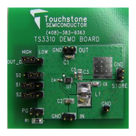
COMPONENT LIST
DESIGNATION
L1
C6
C2, C3
C4, C5
C1
R1
U1
IN, STORE, OUT, PG,
GND (4)
S0, S1, S2, OUT_ON
Figure 1. TS3310DB Top View
Arrow.com.
Downloaded from
, 0.9-3.6V
, Selectable 1.8-5V
Q
IN
QTY
DESCRIPTION
1
10µH ±10% Wire-wound
(Unshielded, 1210)
CBC3225T100KR
1
220pF ±5% capacitor
(C0G, 50V, 0805)
CL21C221JBANFNC
2
10µF ±10% capacitor
(X5R, 16V, 0805)
EMK212BJ106KG-T
2
0.1µF ±10% capacitor
(X7R, 16V, 0402)
EMK105B7104KV-F
1
0.1µF ±10% capacitor
(X7R, 50V, 0805)
08055C104KAT2A
1
3.3MΩ ± 1% (0805)
CRCW08053M30FKEA
1
TS3310
8
Test points
4
Jumper
TS3310 Demo Board
Instant-On
OUT
FEATURES
Input Voltage Range: 0.9V- 3.6V
Jumper Selectable Output Voltages: 1.8V,
2.1V, 2.5V, 2.85V, 3V, 3.3V, 4.1V, and 5V
OUT Enable/Disable Jumper
10µH Inductor, 900mA I
(Taiyo Yuden: CBC3225T100KR)
DESCRIPTION
The TS3310 is a low power boost converter with an
industry leading low quiescent current of 150nA,
enabling ultra long battery life in systems running
from a variety of battery sources. The TS3310 steps
up input voltages from 0.9V to 3.6V to eight
selectable output voltages ranging from 1.8V to 5.0V.
The TS3310 includes two output options, one being
an always-on storage output while the additional
output is an output load switch that is designed to
burst-on loads in a low duty cycle manner.
The TS3310 output voltage can be set via jumpers
S0, S1, and S2. Both the STORE and OUT output
can be monitored along with the power good output
VGOOD. Jumper OUT_ON is available to disable or
enable the OUT output.
Product data sheet and additional documentation can
be found at www.silabs.com.
ORDERING INFORMATION
Order Number
TS3310DB
Figure 2. TS3310DB Bottom View
© 2014 Silicon Laboratories, Inc. All rights reserved.
TM
Boost Converter
SAT
Description
TS3310 Demo Board
10µH Operation
Page 1
Advertisement

Subscribe to Our Youtube Channel
Related Manuals for Silicon Laboratories TS3310DB


Summary of Contents for Silicon Laboratories TS3310DB
- Page 1 Test points GND (4) Order Number Description TS3310 Demo Board S0, S1, S2, OUT_ON Jumper TS3310DB 10µH Operation Figure 1. TS3310DB Top View Figure 2. TS3310DB Bottom View Page 1 © 2014 Silicon Laboratories, Inc. All rights reserved. Arrow.com. Downloaded from...
- Page 2 TS3310 Demo Board DESCRIPTION The TS3310 demo board is configured for 3V output by default. With a 1.2V input voltage, the TS3310DB The TS3310DB is configured for 10µH inductor which is configured for 10µH operation can supply a operation and includes a 220pF C...
- Page 3 Required Equipment TS3310-10DB, configured 10µH operation, connect a 75Ω resistor from STORE to TS3310DB GND. 1.2V Battery or 1.2V Power Supply 7) To measure the STORE output current, connect an Ammeter in series between the 75Ω Resistor Three Digital Multimeters and GND.
- Page 4 TS3310 Demo Board Figure 4. TS3310DB Top Layer #1 Figure 5. TS3310DB Top Layer #2 Figure 6. TS3310DB Top Layer #3 Figure 7. TS3310DB Bottom Layer #1 Figure 8. TS3310DB Bottom Layer #2 Figure 9. TS3310DB Bottom Layer #3 Page 4 Silicon Laboratories, Inc.
Need help?
Do you have a question about the TS3310DB and is the answer not in the manual?
Questions and answers