Table of Contents
Advertisement
Si47
E
XX
VALUATION
1. Introduction
Thank you for purchasing the Silicon Laboratories, Inc. Si47xx Evaluation Board (EVB). The EVB and associated
software have been designed to speed up the overall development process. We look forward to working with you,
and have posted support articles, answers to frequently asked questions, and application notes at
www.mysilabs.com. Table 1 describes all of the available products and features in the Si47xx family.
Part Number
General Description
Si4700
FM Receiver
Si4701
FM Receiver with RDS
Si4702
FM Receiver
Si4703
FM Receiver with RDS
Si4704
FM Receiver
Si4705
FM Receiver with RDS
Si4706
High Performance RDS Receiver
Si4707
WB Receiver with SAME
Si4710
FM Transmitter
Si4711
FM Transmitter with RDS
Si4712
FM Transmitter with RPS
Si4713
FM Transmitter with RDS & RPS
Si4720
FM Transceiver
Si4721
FM Transceiver with RDS
Si4730
AM/FM Receiver
Si4731
AM/FM Receiver with RDS
Si4734
AM/SW/LW/FM Receiver
Si4735
AM/SW/LW/FM Receiver with RDS
Si4736
AM/FM/WB Receiver
Si4737
AM/FM/WB Receiver with RDS
Si4738
FM/WB Receiver
Si4739
FM/WB Receiver with RDS
Si4740
AM/FM Receiver
Si4741
AM/FM Receiver with RDS
Si4742
AM/LW/FM/WB Receiver
Si4743
AM/LW/FM/WB Receiver with RDS
Si4749
High-Performance RDS Receiver
Rev. 0.4 3/08
Si4706, Si4707, and Si474x are under non-disclosure agreement (NDA). Refer to Si4706/07/4x-EVB User's Guide for information on these parts.
B
U
OA RD
Table 1. Product Family Function
Copyright © 2008 by Silicon Laboratories
Si 47xx-EVB
'
G
SER
S
UIDE
LW
LW
4x4
4x4
3x3
3x3
3x3
3x3
3x3
3x3
3x3
3x3
3x3
3x3
3x3
3x3
3x3
3x3
3x3
3x3
3x3
3x3
3x3
3x3
4x4
4x4
4x4
4x4
4x4
Si47xx-EVB
Advertisement
Table of Contents

Related Manuals for Silicon Laboratories Si47xx-EVB Series


Summary of Contents for Silicon Laboratories Si47xx-EVB Series
-
Page 1: Introduction
UIDE 1. Introduction Thank you for purchasing the Silicon Laboratories, Inc. Si47xx Evaluation Board (EVB). The EVB and associated software have been designed to speed up the overall development process. We look forward to working with you, and have posted support articles, answers to frequently asked questions, and application notes at www.mysilabs.com. -
Page 2: Table Of Contents
Si47xx-EVB ABLE O F ONTENTS 1. Introduction .............1 2. - Page 3 Si47xx-EVB 8. AM Receiver GUI ............70 8.1.
- Page 4 Si47xx-EVB This user's guide contains information related to only the Si47xx EVBs itemized in Table 2. Table 2 serves as a quick reference guide for the sections of interest for your EVB. Sections 1, 4, 9, and 10 of the document apply to all EVBs.
- Page 5 Si47xx-EVB Quick start guide The Si471x EVB kit ships with the following items: Si471x FM Transmitter customer welcome and evaluation letter Si47xx Baseboard revision 1.3 or later Si471x/2x Daughterboard revision 1.2 or later with Si471x EVB Characterization Report USB cable RCA cable Adapters—BNC plug to RCA jack 9 V battery...
- Page 6 Si47xx-EVB The Si472x EVB kit ships with the following items: Si472x FM Transceiver customer welcome and evaluation letter Si47xx Baseboard revision 1.3 or later Si471x/2x Daughterboard revision 1.2 or later with Si472x EVB Characterization Report USB cable RCA cable Adapters - BNC plug to RCA jack 9 V battery Headphones Si472x CD including:...
-
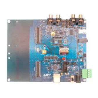
Page 7: Description
Si47xx-EVB 2. Description Si47xx EVB consists of a baseboard, a daughtercard with the Si47xx part pre-mounted, and, if applicable, an antenna card. The baseboard is common and shared among all Si47xx EVBs. The following sections refer to both the images in the figures and the silkscreen on the Si47xx EVB. Please refer to both when using this guide. 2.1. - Page 8 Si47xx-EVB Baseboard audio I/O connectors: RCA output Line output Baseboard clock connectors/devices: 32.768 kHz crystal oscillator Solder bump: select internal RCLK from oscillator Ext RCLK SMA connector input Jumper: Enable or Disable Int RCLK Baseboard MCU connectors/devices: C8051F342 MCU USB connector to communicate with the MCU JTAG connector for the MCU Push button to reset the MCU LED to confirm power supply to the MCU...
- Page 9 Si47xx-EVB The Si47xx EVB can be powered using one of the following power supply options: 1. USB power supply via J79 2. External dc (Ext DC) power supply via power jack J78 or battery via J77 3. Three separate power supplies (Vdd, Vio, Vmcu) via terminal block J76 The EVB has three supply rails: Vdd, Vio, and Vmcu.
- Page 10 Figure 5. MCU Block Diagram The Si47xx EVB uses a Silicon Laboratories' C8051F342 microcontroller to control the Si47xx and to provide USB connectivity from the host PC (via connector J79). The LED D1 illuminates to confirm that power is being properly supplied to the C8051F342 and firmware has loaded.
- Page 11 Si47xx-EVB 2.1.3. Reference Clock Daughterboard Jumper Si47xx 32.768 kHz DIS_INT_RCLK INT RClk Jumper RCLK INT_RCLK EXT_RCLK RClk Figure 6. Reference Clock Block Diagram The Si47xx accepts a 32.768 kHz reference clock at the RCLK pin. On the EVB, this clock is provided by a precision crystal oscillator.
- Page 12 Si47xx-EVB The EVB supports three different kinds of configurations for the FM transmitter: Analog In to Analog In Analog In to Digital In Digital In to Digital In Analog In to Analog In: This configuration provides a way for the user to evaluate the analog audio input for FM transmission.
- Page 13 Si47xx-EVB IMPORTANT: Jumper Settings Because of the many possibilities available to configure the EVB, ensure that these four jumpers are set accordingly: 1. J41: GPO3/DCLK setting 2. J44: TX/RX setting for Audio1 I/O (automatically set by the GUI for baseboard 1.3 and later) 3.
-
Page 14: Si47Xx Daughtercards
Si47xx-EVB 2.2. Si47xx Daughtercards 2.2.1. Si471x/2x Daughtercard Figure 8. Si471x/2x Daughterboard Connectors and Devices Daughterboard Connectors and Components: Si472x FM Transceiver or Si470x FM Receiver or Si471x FM Transmitter Tuning Inductor 0 Ω resistor to connect FM TX output to 10 cm trace built-in antenna 2 pF capacitor to connect FM TX output to J1 SMA connector 50 Ω... - Page 15 Si47xx-EVB Figure 9. Fully Assembled Si471x/2x EVB Si470x/1x/2x EVBs use Si471x/2x daughtercard with different population options depending on the individual Si470x/1x/2x part. Please refer to individual Bill of Materials for each board. 2.2.1.1. FM Transmitter The Si471x/2x (U1) and its bypass capacitors and tuning inductor (L2) are located on the daughtercard. The FM transmit output can be configured in three different ways: Built-in antenna External antenna...
- Page 16 Si47xx-EVB 2.2.1.2. FM Receiver As an FM receiver, the FM input can be configured in three ways: Built-in antenna Headphone antenna RF input Built-In Antenna The built-in PCB trace antenna is available by default. Headphone Antenna To use a headphone antenna, connect the headphone to the headphone jack J29 that is on the daughtercard. The daughtercard also includes a headphone amplifier, which enables the user to listen to the audio output via the headphone connected to J29.
- Page 17 Si47xx-EVB Daughterboard connectors and components: SMA connector for AM test circuit Header for antenna interface connection Headphone jack SMA connector for FM test circuit 270 nH inductor for FM input Si473x AM/FM/SW Weather Band Receiver chip Vdd bypass capacitor FM test circuit ac coupling capacitor AM input ac coupling capacitor FM input ac coupling capacitor AM test circuit ac coupling capacitor...
- Page 18 Si47xx-EVB Figure 12. Fully Assembled Si473x-EVB with Ferrite Antenna Card The daughtercard implements the Si473x AM/FM receive solution. The AM interface allows the user the option to choose between a ferrite loop stick antenna and an airloop antenna. The user can also configure the daughterboard to use the AM test circuit for Si473x AM characterization.
- Page 19 Si47xx-EVB 2.2.4. Antenna Interfaces 2.2.4.1. AM Antenna Interface Figure 13. Antenna Board Options—SL4X30MW100T Ferrite, SL5X7X100MW70T Ferrite, and SL9X5X4MWTF Airloop The user has the flexibility of choosing one of the two available antenna options. The user can either decide to use the airloop antenna or the ferrite loop stick antenna.
- Page 20 Si47xx-EVB 2.2.4.1.1. Ferrite Loop Stick Antenna A ferrite loop stick antenna can be used with the Si473x by connecting the ferrite antenna board as shown in Figure 14. Head Phone Jack/FM Buffers Antenna FM Input Analog SMA IN Test Audio Out Circuit FM Input LOUT...
- Page 21 Si47xx-EVB 2.2.4.1.2. Airloop Antenna An airloop antenna can be used by connecting the airloop antenna board as shown in Figure 15. Head Phone Jack/FM Buffers Antenna FM Input Analog SMA IN Test Audio Out Circuit FM Input LOUT ROUT RFGND Airloop Antenna Si473x Board...
- Page 22 Si47xx-EVB 2.2.4.2. FM Antenna Interface Head Phone Jack/FM Buffers Antenna FM Input Analog SMA IN Test Audio Out Circuit FM Input LOUT ROUT RFGND Si473x Digital* SMA IN Test AM Input Audio Out Circuit GPO3/DCLK 17 DOUT *Note: Si4731/5/7/9 only Daughterboard with FW 2.0 or higher Figure 16.
- Page 23 Si47xx-EVB 2.2.4.3. SW and Weather Band Antenna Interface Figure 17. SW/WB Antenna Card (SW population option shown) Figure 18. Fully Assembled Si473x-EVB with SW/WB Antenna Card The BNC connector, J2, will be used to connect a whip antenna for shortwave, FM, and weather band reception. For SW reception, switch S1 must be in the SW position.
- Page 24 Si47xx-EVB 2.2.5. Test Circuit Interfaces 2.2.5.1. AM/LW/SW Test Circuit Interface Head Phone Jack/FM Buffers Antenna FM Input Analog SMA IN Test Audio Out Circuit FM Input LOUT ROUT RFGND Si473x Digital* SMA IN Test AM Input Audio Out Circuit GPO3/DCLK 17 DOUT *Note: Si4731/5/7/9 only Daughterboard...
- Page 25 Si47xx-EVB 2.2.5.2. FM/Weather Band Test Circuit Interface Head Phone Jack/FM Buffers Antenna FM Input Analog SMA IN Test Audio Out Circuit FM Input LOUT ROUT RFGND Si473x Digital* SMA IN Test AM Input Audio Out Circuit GPO3/DCLK 17 DOUT *Note: Si4731 only with Daughterboard FW 2.0 or higher Figure 20.
-
Page 26: Recommended Hardware Setup
Si47xx-EVB 3. Recommended Hardware Setup The Si47xx-EVB can be configured for FM transmit, FM receive, weather band receiver, or AM/SW receive. The following is a description of how to correctly configure the device for either mode of operation. 3.1. Hardware Setup for FM Transmitter Test Analog Audio Analyzer... -
Page 27: Hardware Setup For Fm Or Weather Band Receiver Test
Si47xx-EVB 3.2. Hardware Setup for FM or Weather Band Receiver Test Audio Generator Analyzer SMA Cable RCA Cable J28 or J26 Optical FM IN RCA OUT RCA IN Cable Si47xx Jumpers Daughterboard Setting S/PDIF DCLK GPIO3 J44 J45 Note: J44 and J45 are automatically configured in EVB Rev1.3 and later Si47xx... -
Page 28: Hardware Setup For Am Receiver Test
Si47xx-EVB 3.3. Hardware Setup for AM Receiver Test Audio Analyzer RCA Cable J28 or J26 Optical FM IN RCA OUT RCA IN Cable Si473x Jumpers Daughterboard Generator Setting S/PDIF DCLK SMA Cable GPIO3 J44 J45 Note: J44 and J45 are automatically configured in EVB Rev1.3 and later Si47xx... -
Page 29: Getting Started-Software Installation
Windows XP and Windows 2000. To install, insert the Silicon Laboratories Si47xx CD into the host machine CD drive and launch Windows Explorer. Open the CD to explore the contents in a window like the one shown in Figure 24. -
Page 30: Fm Transmitter Gui
Si47xx-EVB 5. FM Transmitter GUI The first Si47xx window is the Initialization window as shown in Figure 26. Select the FM transmitter function. As an FM transmitter, there are three audio input settings available: Analog Input Analog to Digital Input Digital Input 5.1. -
Page 31: Configuring The Si47Xx As An Fm Transmitter Using Digital Audio With Analog Audio
Si47xx-EVB 5.2. Configuring the Si47xx as an FM Transmitter Using Digital Audio with Analog Audio Source This mode configures the Si47xx to receive digital audio input at pin 13 and 14 (DIN and DFS), but the user still provides an analog audio source to the EVB. It is useful for a user who wants to test digital input on the Si47xx but does not have a digital audio source. -
Page 32: Configuring The Si47Xx As An Fm Transmitter Using Digital Audio With Spdif Digital
Si47xx-EVB 5.3. Configuring the Si47xx as an FM Transmitter Using Digital Audio with SPDIF Digital Source This mode configures the Si47xx to receive digital audio input at pin 13 and 14 (DIN and DFS) when the user has an SPDIF digital audio source. The SPDIF source is converted to PCM digital audio by the SPDIF translator. Refer to Figure 33, “SPDIF Settings Property Window,”... -
Page 33: Fm Transmitter Main Window
Si47xx-EVB 5.4. FM Transmitter Main Window The FM transmitter main window will appear after initialization. Figure 29. FM Transmitter Main Window Table 4. FM Transmitter Main Window Descriptions Description Range 1 Transmit frequency display. Enter the desired FM transmit frequency in this window. 76–108 MHz 2 Transmit voltage display. - Page 34 Si47xx-EVB Table 4. FM Transmitter Main Window Descriptions (Continued) Description Range 11 RDS Deviation. Enter the desired RDS deviation in this window (Si4721 only). 0–7.5 kHz 12 Total Deviation. This is an indicator only displaying the sum of the audio, pilot and RDS 0–187.5 kHz deviation.
-
Page 35: Fm Transmitter Settings (Analog Mode) Property Window
Si47xx-EVB 5.5. FM Transmitter Settings (Analog Mode) Property Window → → FM transmitter settings are configured by selecting Windows Properties FM Transmitter Settings when analog mode is selected in the initialization window. Figure 30. FM Transmitter Settings in Analog Mode Property Window Table 5. - Page 36 Si47xx-EVB Table 5. FM Transmitter Settings in Analog Mode Property Window Descriptions (Continued) Item Description Range Audio Level High 0–65535 Set the duration for the audio level high before an interrupt is Duration (mSec) generated. Line Input 190 mVp, 301 mVpk, The Si47xx has four attenuator settings (636, 416, 301, and Attenuation 416 mVp, 636 mVpk...
-
Page 37: Fm Transmitter Settings (Digital Mode) Property Window
Si47xx-EVB 5.6. FM Transmitter Settings (Digital Mode) Property Window → → FM transmitter settings are configured by selecting Windows Properties FM Transmitter Settings when CODEC or SPDIF mode is selected in the initialization window. Figure 31. FM Transmitter Settings in Digital Mode Property Window Table 6. - Page 38 Si47xx-EVB Table 6. FM Transmitter Settings in Digital Mode Property Window Descriptions (Continued) Item Description Range Digital Format Left-Justified, I Sets I S of left justified digital format. DSP (MSB on first DCLK), or DSP (MSB on second DCLK) Digital Sample 8, 16, 20, 24 bits Select the precision of the digital audio input.
-
Page 39: Codec Settings
Si47xx-EVB 5.7. CODEC Settings → → CODEC settings are configured by selecting Windows Properties CODEC Settings when CODEC mode is selected in the initialization window. Figure 32. CODEC Settings Property Window Table 7. CODEC Settings Property Window Descriptions Item Description Range CODEC Precision 16, 20, 24 bits... -
Page 40: Spdif Settings
Si47xx-EVB 5.8. SPDIF Settings → → SPDIF settings are configured by selecting Windows Properties SPDIF Settings when digital SPDIF mode is selected in the initialization window. Figure 33. SPDIF Settings Property Window Table 8. SPDIF Settings Property Window Descriptions Item Description Range SPDIF Output Format Select the SPDIF digital audio format between I... -
Page 41: Fm Transmitter Receive Power Scan Window
Si47xx-EVB 5.9. FM Transmitter Receive Power Scan Window The Receive Power Scan window enables the user to scan the entire FM band to find one or more candidate channels on which to transmit, where candidate channels are defined as those with the lowest received power. →... -
Page 42: Fm Transmitter Radio Data Service (Rds)
Si47xx-EVB 5.10. FM Transmitter Radio Data Service (RDS) The RDS/RBDS feature is available with the Si4711/13/21. This user guide assumes that the user is already familiar with the RDS/RBDS standard. If necessary, the user may refer to the following documents to become familiar with the RDS/RBDS standard. - Page 43 Si47xx-EVB Figure 36. RDS Transmit Window Table 9. RDS Transmit Window Descriptions Item Description General RDS/RBDS Selection Select either RDS format (Europe) or RBDS format (US). Program Type (PTY) Select the available Program Type (PTY) from the pulldown menu. PTY Dynamic Select whether the PTY will be dynamic or static.
- Page 44 Si47xx-EVB Table 9. RDS Transmit Window Descriptions Item Description Stereo Part of RDS Group Type 0 (PS): Enter whether the transmitted audio is Stereo or Mono. Audio Compression Part of RDS Group Type 0 (PS): Enter whether the Audio Compression is On or Off. Traffic Program Part of RDS Group Type 0 (PS): Enter whether Traffic Program is available or not.
- Page 45 Si47xx-EVB There are 16 different group types in the RDS/RBDS standard, and for every group the following information is always transmitted: 1. Program Identification (PI) 2. Program Type (PTY) The Si47xx GUI makes it easy to send data in three of the following group types: 1.
- Page 46 Si47xx-EVB 5.10.1. Basic The RDS Transmit Window is divided into three categories: 1. General 2. Program Service 3. Buffers In the basic section, we will cover two out of the three categories: the General and Program Service. In the General category, the user can set the PI and PTY data.
- Page 47 Si47xx-EVB 5.10.2. Intermediate In the intermediate section, we will cover the buffers category of sending the RDS data with the device, in particular we will send Group Type 2 (Radio Text) and Group Type 4 (Clock Time). The following diagram shows a step-by-step procedure to send the buffers data in addition to the General and Program Service data covered in the basic section.
- Page 48 Si47xx-EVB 5.10.3. Advanced In the advanced section, we will cover the remaining RDS topics. Figure 39. Advanced RDS Sending Illustration 1. Dynamic: This tells whether the PTY code is static or dynamic. 2. Alternate Frequency: This provides the ability to inform the receiver of a single alternate frequency. This field is transmitted along with the Group Type 0 (PS).
-
Page 49: Fm Transmitter Register Map Window
Si47xx-EVB 5.11. FM Transmitter Register Map Window The register map window allows the user to manually program the device by sending commands to the chip. Refer → to “AN332: Si47xx Programming Guide” to manually program the device. Clicking on Windows Register Map will launch the Register Map Window as shown in Figure 40. -
Page 50: Fm Receiver Gui
Si47xx-EVB 6. FM Receiver GUI The first Si47xx window is the Initialization window as shown in Figure 41. Select the FM receiver function. As an FM receiver, analog audio out is available on pins 13 and 14. 6.1. Configuring the Si47xx as an FM Receiver Select the device, busmode, firmware revision, and initial part settings and then click Initialize. -
Page 51: Fm Receiver Main Window
Si47xx-EVB 6.2. FM Receiver Main Window The FM receiver main window will appear after initialization. Figure 42. FM Receiver Main Window Rev. 0.4... - Page 52 Si47xx-EVB Table 10. FM Receiver Main Window Descriptions Name Descriptions Tune/Seek Tune Down (<), Tune Up (>) buttons execute a single channel step according to the channel spacing setting. The channel spacing setting can be set in the property window. Seek down (<<), Seek Up (>>) buttons execute a seek up or down to the next received FM signal meeting or exceeding the seek settings within the selected band.
-
Page 53: Fm Receiver Settings Property Window
Si47xx-EVB 6.3. FM Receiver Settings Property Window → → Select Window Properties FM Receiver Settings. Figure 43. FM Receiver Settings Property Window Rev. 0.4... - Page 54 Si47xx-EVB Table 11. FM Receiver Settings Property Window Descriptions Items Description Range Antenna Type Receive antenna selection Headphone or short antenna Band Frequency band US/Europe: 87.5–108 MHz Japan: 76–90 MHz Japan Wide: 76–108 MHz De-emphasis Selects de-emphasis of 50 µs or 75 µs. 50 µs, 75 µs Digital DCLK Falling Edge ON uses falling edge of DCLK for sampling.
- Page 55 Si47xx-EVB Table 11. FM Receiver Settings Property Window Descriptions (Continued) Items Description Range Soft Mute SNR Threshold SNR threshold level used to engage soft mute. 0–15 dB (dB) Spacing Channel spacing 50, 100, or 200 kHz Stereo Blend Mono RSSI threshold below which the tuner blends into 0–127 dB Threshold (dB) full mono.
-
Page 56: Codec And Spdif Settings
Si47xx-EVB 6.4. CODEC and SPDIF Settings Si47xx-EVB baseboard has a Codec and an SPDIF translator for digital audio output. For tuners with digital audio option, you can set properties for the Codec and SPDIF through the GUI. These settings can be used with AM or FM tuners that have digital audio enabled. -
Page 57: Fm Receiver Rds Window
Si47xx-EVB 6.5. FM Receiver RDS Window The FM receive RDS window allows the user to view program service, program type, PI code, radio text, clock, group error rate, sync time and display times, an alternate frequency list, and group statistics. Select →... - Page 58 Si47xx-EVB Table 13. FM Receiver Settings RDS Window Descriptions Items Description Radio Data Service PS: Program Service Indicator (8 characters). RT: Radio Text Indicator (64 characters). CT: Clock Indicator showing time, day, and date. Group Error Rate indicates the percentage of uncorrectable groups received. PTY: Program Type Indicator PI: PI Code Indicator Sync Times...
- Page 59 Si47xx-EVB Figure 46. RDS Group Counters Window Rev. 0.4...
-
Page 60: Fm Receiver Rds Settings
Si47xx-EVB 6.6. FM Receiver RDS Settings → → RDS settings are configured by selecting Windows Properties FM Receiver RDS Settings. Figure 47. FM Receiver RDS Settings Window Rev. 0.4... - Page 61 Si47xx-EVB Table 14. FM Receiver RDS Settings Window Descriptions Item Description Range RDS State Enables and disables RDS. On, Off RDS (RT and PS) Error Checking Selects GUI error checking level. Minimum, Mid-Range, Maximum Minimum displays text as received. Mid-range requires two duplicate buffers before displaying text.
-
Page 62: Fm Ui Settings
Si47xx-EVB 6.7. FM UI Settings Figure 48. FM UI Settings Property Window Table 15. FM UI Settings Property Window Descriptions Hems Description Range 0.2–4.0 seconds Update Rate (sec) The time span when the UI gets status information from the part. 1–10 seconds Scan Time 1 (sec) In log band scan, the time between seeking and... -
Page 63: Fm Receiver Rssi/Snr Graph Window
Si47xx-EVB 6.8. FM Receiver RSSI/SNR Graph Window The RSSI/SNR Graph Window allows the user to plot RSSI and SNR across the FM band. Bitmap data can be → → saved to file by selecting File Save as Bitmap and tabulated data can be saved to file by selecting File Save to .csv. -
Page 64: Fm Receiver Register Map Window
Si47xx-EVB 6.9. FM Receiver Register Map Window The register map window allows the user to manually program the device by sending commands to the device. Refer to "AN332: Si47xx Programming Guide" to manually program the device. Figure 50. FM Receiver Register Map Window Rev. -
Page 65: Weather Band Gui
Si47xx-EVB 7. Weather Band GUI The first Si47xx window is the Initialization window as shown in Figure 51. Select the Weather Band function. For weather band, analog audio out is available on pins 13 and 14. 7.1. Configuring the Si4736/37/38/39 as Weather Band Receiver Select the device, busmode, firmware revision, and initial part settings and then click Initialize. -
Page 66: Weather Band Main Window
Si47xx-EVB 7.2. Weather Band Main Window The weather band main window will appear after initialization. Figure 52. Weather Band Main Window Table 17. Weather Band Main Window Descriptions Name Descriptions RSSI/SNR/ The RSSI indicator displays the RSSI of the signal in dBuV. The SNR indicator displays the SNR of the received signal in dB. -
Page 67: Weather Band Settings Property Window
Si47xx-EVB 7.3. Weather Band Settings Property Window → → Select Window Properties WB Receiver Settings. Figure 53. Weather Band Receiver Settings Property Window Table 18. Weather Band Receiver Settings Property Window Descriptions Items Description Range Reference Clock Frequency (Hz) This field is used to specify the frequency of the reference 31130–34406 Hz clock. -
Page 68: Weather Band Receiver Rssi/Snr Graph Window
Si47xx-EVB 7.4. Weather Band Receiver RSSI/SNR Graph Window The RSSI/SNR Graph Window allows the user to plot RSSI and SNR across the weather band. Bitmap data can be → → saved to file by selecting File Save as Bitmap and tabulated data can be saved to file by selecting File Save to .csv. -
Page 69: Weather Band Receiver Register Map Window
Si47xx-EVB 7.5. Weather Band Receiver Register Map Window The register map window allows the user to manually program the device by sending commands to the device. Refer to "AN332: Si47xx Programming Guide" to manually program the device. Figure 55. Weather Band Receiver Register Map Window Rev. -
Page 70: Am Receiver Gui
Si47xx-EVB 8. AM Receiver GUI 8.1. AM Receiver Initialization The first Si473x window is the Initialization window as shown in Figure 56. On the function drop-down menu, select the function of the Si473x as an AM Receiver. Select the device, busmode, firmware revision, and initial part settings and then click Initialize. -
Page 71: Am Receiver Main Window
Si47xx-EVB 8.2. AM Receiver Main Window The AM receiver main window will appear after initialization. Figure 57. AM Receiver Window Table 20. AM Receiver Window Descriptions Name Description Tune/Seek Tune Down (<), Tune Up (>) buttons execute a single channel step according to the channel spacing setting. -
Page 72: Am Receiver Property Settings Window
Si47xx-EVB 8.3. AM Receiver Property Settings Window Figure 58. AM Receiver Settings Property Window Rev. 0.4... - Page 73 Si47xx-EVB Table 21. AM Receiver Property Window Descriptions Name Description Range Channel Filter 1, 2, 3, 4, 6 kHz Channel Filter allows the user to select the bandwidth of the bandpass channel filter. De-emphasis On/Off De-emphasis filter setting allows the user to select whether to turn on/ off the de-emphasis filter.
- Page 74 Si47xx-EVB Table 21. AM Receiver Property Window Descriptions (Continued) Name Description Range Soft Mute Rate 0–1109.5 dB in units of Soft mute rate specifies how quickly to mute the output when the signal (dB/s) 4.35 dB level falls below the threshold specified for soft mute or how quickly to come out of soft mute when the level is above the threshold.
-
Page 75: Am Receiver Rssi/Snr Graph Window
Si47xx-EVB 8.4. AM Receiver RSSI/SNR Graph Window The RSSI/SNR graph window allows the user to plot RSSI and SNR across the AM band. Bitmap data can be → → saved to file by selecting File Save as Bitmap and tabulated data can be saved to file by selecting File Save to .csv. -
Page 76: Am Receiver Register Map Window
Si47xx-EVB 8.5. AM Receiver Register Map Window The register map window allows the user to manually program the device by sending commands to the device. Refer to "AN332: Si47xx Programming Guide" to manually program the device. Figure 60. Register Map Window Rev. -
Page 77: Using The Evb With A 9 V Battery
Si47xx-EVB 9. Using the EVB with a 9 V Battery The EVB can be used with a 9 V battery that allows the user to disconnect the board from the computer for evaluating the Si47xx. Follow the guidelines listed below to use your EVB with a 9 V battery. 1. -
Page 78: Debugging Guidelines For Si47Xx Evb
Si47xx-EVB 10. Debugging Guidelines for Si47xx EVB Table 23. Debugging Guidelines for Si47xx EVB Mode Symptom Solution Configuration EVB not recognized If the EVB is not recognized by the PC, remove the USB connection and reconnect. Ensure the EVB is recognized by the PC by right-clicking on My Computer and selecting Properties→Hardware→Device Manager. - Page 79 Si47xx-EVB Table 23. Debugging Guidelines for Si47xx EVB FM Transmit Poor transmit audio Increase the RF level. quality Increase the audio deviation level. Change the RF frequency to a channel with less interference. The RPS feature can be used to find candidate frequencies. Rev.
-
Page 80: Bill Of Materials
Si47xx-EVB 11. Bill of Materials Table 24. Si47xx-EVB Baseboard Rev 1.4—Bill of Materials Item REFDES Description Value Mfg/Vendor Mfg/Vendor_PN 2.1mm power plug CONN_PJ-01 C1,C2,C4,C11,C13,C28,C31,C33, CAP,SM,0402,0.1UF,10% 0.1UF VENKEL C0402X7R160- C34,C35,C36,C39,C40,C42,C43, 104KNE C46,C50,C52,C54,C55,C57,C61, C62,C68,C71,C73,C74 RADIAL CAP 4.7UF Kemet T350B475K016AS CAP,SM,0805 0.1UF CAP,SM,7343,15UF,10% 15UF VISHAY 293D156X9020D2T... - Page 81 Si47xx-EVB Table 24. Si47xx-EVB Baseboard Rev 1.4—Bill of Materials (Continued) Item REFDES Description Value Mfg/Vendor Mfg/Vendor_PN R8,R9,R20,R48,R49,R50,R51,R52, RES,SM,0402 VENKEL CR0402-16W-000T R53,R54,R55,R56,R57,R58,R59, R60,R62,R63,R68,R69,R71,R72, R75,R77,R79,R81,R82,R91 RES,SM,0402 22.1 VENKEL CR0402-16W-22R1FT R5,R7,R10,R11,R29 RES,SM,0402 KOA SPEER RK73H1ELTP1002F R12,R13 RES,SM,0402 5.6K KOA SPEER RK73H1ELTP5601F RES,SM,0402 VENKEL CR0402-16W-330GT R17,R27,R36,R19 RES,SM,0402...
- Page 82 Si47xx-EVB Table 24. Si47xx-EVB Baseboard Rev 1.4—Bill of Materials (Continued) Item REFDES Description Value Mfg/Vendor Mfg/Vendor_PN XTAL,12.288MHZ,18PF CITIZEN AMER- CS10-12.288MABJ-UT ICA CORP R30,R32,R35,R37,R39,R40,R41, Res,sm,0402 49.9 Venkel CR0402-16W-49R9FT R42,R92,R93,R94,R95 4P Plug 180Deg terminal block MOUSER 651-1803594 ELECTRONICS U23, U26 Diode,SM,SD103AW,Shottkey Diodes SD103AW-7 diode Screw Pan 440x3/4...
- Page 83 Si47xx-EVB Table 25. Si471x/2x-EVB Daughtercard (Rev 1.4)—Bill of Materials ITEM REFDES DESCRIPTION VALUE MFG/Vendor MFG/Vendor_PN 2 C4,C6 CAP,SM,0402,X7R 22PF MURATA GRM185R71E220KA61D 1 C2 CAP,SM,0402,X7R 22NF MURATA GRM185R71E223KA61D 2 C7,C10 CAP,SM,0402,X7R 0.1UF MURATA GRM185R71C104KA88D 2 C3,C5 CAP,SM,0603,X7R 0.47UF VENKEL C0603X7R160-474KNE 2 C1,C9 CAP,SM,0603,X7R MURATA GRM185R71E102KA61D...
- Page 84 Si47xx-EVB Table 26. Si473x-EVB Daughtercard Rev 1.4—Bill of Materials ITEM REFDES DE SCRIPTION VALUE MFG/V endor MFG/V endor_PN 2 C1,C7 CA P,SM,0402,X7R 0.1UF MURATA GRM155R71C104KA88D 1 C2 CA P,SM,0402,X7R 22NF MURATA GRM155R71E223KA61D 3 C9,C10,C11 CA P,SM,0402,X7R 100PF MURATA GRM1555C1H101JZ01D 3 C3,C5,C12 CA P,SM,0603,X7R VENKEL C0603C0G500-103JNE...
- Page 85 Si47xx-EVB Table 27. Si4730 Ferrite Medium Antenna Rev 1.2—Bill of Materials ITEM QTY REFDES DESCRIPTION VALUE M FG/Ve ndor M FG/Ve ndor_PN 1 J4 Socket Header, TH, Friction notch SAMTEC SSW-112-02-G-P-RA 1 U1 Medium Ferrite Core SiLabs SL4X30MW110T 1 A1 PCB, Ferrite Antenna Board Zip Tie 6in HellermannTyton...
- Page 86 Si47xx-EVB Table 30. Si473x SW/WB Antenna—Bill of Materials ITEM REFDES DESCRIPTION V ALUE M FG/V e ndor CA P,SM,0402,C0G 18pF V ENKEL CA P,SM,0402,C0G 33pF V ENKEL Socket Header, TH, Friction notch SA MTEC BNC,EDGE-MOUNT, GOLD PLA TED MOUSER Large Ferrite Core SiLabs IND,SM,0603 470nH MURA TA...
-
Page 87: Schematics
Si47xx-EVB 12. Schematics 12.1. Si47xx-EVB Baseboard Rev 1.4 Rev. 0.4... - Page 88 Si47xx-EVB Rev. 0.4...
- Page 89 Si47xx-EVB Rev. 0.4...
- Page 90 Si47xx-EVB Rev. 0.4...
- Page 91 Si47xx-EVB Note: For EN55020 compliance, please add the following components to L-OUT and R-OUT @ J6: 1 µF from C5 x C7 to GND (one for each output), 22.6 Ω in series with C5 x C7 (one for each output). Rev.
- Page 92 Si47xx-EVB Rev. 0.4...
- Page 93 Si47xx-EVB Rev. 0.4...
-
Page 94: Si471X/2X-Evb Daughtercard Rev 1.4
Si47xx-EVB 12.2. Si471x/2x-EVB Daughtercard Rev 1.4 Rev. 0.4... - Page 95 Si47xx-EVB Figure 69. Si471x/2x-EVB Daughtercard (Rev 1.4) Headphone Schematic (applies only to Si470x/2x) Si471x/2x-EVB Daughtercard (Rev 1.4) ships configured for external RCLK, supplied by the Si47xx-EVB Baseboard. To configure for crystal oscillator operation: 1. Remove R5. 2. Remove short at J24. 3.
-
Page 96: Si473X-Evb Daughtercard Rev. 1.4
Si47xx-EVB 12.3. Si473x-EVB Daughtercard Rev. 1.4 Rev. 0.4... - Page 97 Si47xx-EVB Figure 71. Si473x-EVB Daughtercard Rev 1.4 (2 of 2) Si473x-EVB Daughtercard (Rev 1.4) ships configured for external RCLK, supplied by the Si47xx-EVB Baseboard. To configure for crystal oscillator operation: 1. Remove R9. 2. Remove R10. 3. Short J27. 4. Short J28. 5.
-
Page 98: Antenna Card Schematics
Si47xx-EVB 12.4. Antenna Card Schematics 12.4.1. Si473x Ferrite Antenna Card Rev 1.2 Figure 72. Ferrite Antenna Card Rev 1.2 12.4.2. Si473x Air Loop Antenna Card Rev 1.2 Figure 73. Airloop Antenna Card Rev 1.2 Rev. 0.4... - Page 99 Si47xx-EVB 12.4.3. Si473x SW/WB Antenna Card Rev 1.3 Note: If an SW band is selected using the SW/WB Antenna Card, set the varactor to 1 for best performance. LW not supported with SW/WB Antenna Card. Figure 74. Si473x SW/WB Antenna Card Rev 1.3 Rev.
-
Page 100: Layout
Si47xx-EVB 13. Layout 13.1. Si47xx-EVB Baseboard Rev 1.4 Figure 75. Si47xx-EVB Baseboard Rev 1.4—Primary Assembly Silkscreen Figure 76. Si47xx-EVB Baseboard Rev 1.4—Secondary Assembly Silkscreen Rev. 0.4... - Page 101 Si47xx-EVB Figure 77. Si47xx-EVB Baseboard Rev 1.4—Primary Side Figure 78. Si47xx-EVB Baseboard Rev 1.4—Ground Plane Rev. 0.4...
- Page 102 Si47xx-EVB Figure 79. Si47xx-EVB Baseboard Rev 1.4—Power Plane Figure 80. Si47xx-EVB Baseboard Rev 1.4—Secondary Side Rev. 0.4...
-
Page 103: Si471X/2X-Evb Daughtercard Rev 1.4
Si47xx-EVB 13.2. Si471x/2x-EVB Daughtercard Rev 1.4 Figure 81. Si471x/2x-EVB Daughtercard (Rev 1.4)—Primary Assembly Silkscreen Figure 82. Si471x/2xEVB Daughtercard (Rev 1.4)—Secondary Assembly Silkscreen Rev. 0.4... - Page 104 Si47xx-EVB Figure 83. Si471x/2x-EVB Daughtercard (Rev 1.4)—Primary Side Figure 84. Si471x/2x-EVB Daughtercard (Rev 1.4)—Ground Plane Rev. 0.4...
- Page 105 Si47xx-EVB Figure 85. Si471x/2x-EVB Daughtercard (Rev 1.4)—Power Plane Figure 86. Si471x/2x-EVB Daughtercard (Rev 1.4)—Secondary Side Rev. 0.4...
-
Page 106: Si473X-Evb Daughtercard Rev 1.4
Si47xx-EVB 13.3. Si473x-EVB Daughtercard Rev 1.4 Figure 87. Si473x-EVB Daughtercard Rev 1.4 - Primary Assembly Silkscreen Figure 88. Si473x-EVB Daughtercard Rev 1.4 - Secondary Assembly Silkscreen Rev. 0.4... - Page 107 Si47xx-EVB Figure 89. Si473x-EVB Daughtercard Rev 1.4—Primary Side Figure 90. Si473x-EVB Daughtercard Rev 1.4—Ground Plane Rev. 0.4...
- Page 108 Si47xx-EVB Figure 91. Si473x-EVB Daughtercard Rev 1.4—Power Plane Figure 92. Si473x-EVB Daughtercard Rev 1.4—Secondary Side Rev. 0.4...
-
Page 109: Antenna Cards
Si47xx-EVB 13.4. Antenna Cards 13.4.1. Si473x Ferrite Antenna Card Rev 1.2 Figure 93. Si473x Ferrite Antenna Card Rev 1.2—Primary Side Silkscreen Figure 94. Si473x Ferrite Antenna Card Rev 1.2—Secondary Side Silkscreen Rev. 0.4... - Page 110 Si47xx-EVB Figure 95. Si473x Ferrite Antenna Card Rev 1.2—Primary Side Figure 96. Si473x Ferrite Antenna Card Rev 1.2—Secondary Side Rev. 0.4...
- Page 111 Si47xx-EVB 13.4.2. Si473x Air Loop Antenna Card Rev 1.2 Figure 97. Si473x Air Loop Antenna Card Rev 1.2—Primary Side Silkscreen Figure 98. Air Loop Antenna Card Rev 1.2—Secondary Side Silkscreen Rev. 0.4...
- Page 112 Si47xx-EVB Figure 99. Si473x Air Loop Antenna Card Rev 1.2—Primary Side Figure 100. Si473x Air Loop Antenna Card Rev 1.2—Secondary Side Rev. 0.4...
- Page 113 Si47xx-EVB 13.4.3. Si473x SW/WB Antenna Card Rev 1.3 Figure 101. Si473x SW/WB Antenna Card Rev 1.3—Primary Side Silkscreen Figure 102. Si473x SW/WB Antenna Card Rev 1.3—Secondary Side Silkscreen Rev. 0.4...
- Page 114 Si47xx-EVB Figure 103. Si473x SW/WB Antenna Card Rev 1.3—Primary Side Figure 104. Si473x SW/WB Antenna Card Rev 1.3—Secondary Side Rev. 0.4...
-
Page 115: Documentation Change List
Si47xx-EVB OCUMENTATION HANGE Revision 0.1 to Revision 0.2 Updated Product Family in Table 1 on page 1. Updated Si4740/41 Property List in Figure on page 54 and Table 11 on page 54. Clarified varactor recommendation with SW operation using SW/WB Antenna Card. Added instructions for daughtercard configurations with crystal oscillator operation. -
Page 116: Contact Information
Silicon Laboratories products are not designed, intended, or authorized for use in applications intended to support or sustain life, or for any other application in which the failure of the Silicon Laboratories product could create a situation where per- sonal injury or death may occur.
Need help?
Do you have a question about the Si47xx-EVB Series and is the answer not in the manual?
Questions and answers