Table of Contents
Advertisement
Quick Links
Advertisement
Table of Contents

Subscribe to Our Youtube Channel
Related Manuals for NXP Semiconductors BGU8007 GPS LNA EVB


Summary of Contents for NXP Semiconductors BGU8007 GPS LNA EVB
- Page 1 UM10497 User manual for the BGU8007 GPS LNA evaluation board Rev. 1.0 — 5 October 2011 User manual Document information Info Content Keywords LNA, GPS, BGU8007 Abstract This document explains the BGU8007 GPS low noise amplifier evaluation board Arrow.com. Downloaded from...
- Page 2 UM10497 NXP Semiconductors BGU8007 GPS LNA EVB Revision history Date Description 20111005 First Release. Contact information For additional information, please visit: http://www.nxp.com For sales office addresses, please send an email to: salesaddresses@nxp.com UM10497 All information provided in this document is subject to legal disclaimers.
-
Page 3: Introduction
BGU8007 GPS LNA EVB 1. Introduction NXP Semiconductors’ BGU8007 is a low-noise amplifier for GPS receiver applications in a plastic, leadless 6 pin, extremely thin small outline SOT886 package. It has a current of 4.6 mA, a gain of 19 dB and a noise figure of 0.75 dB . -
Page 4: General Description
BGU8007 GPS LNA EVB 2. General description NXP Semiconductors’ BGU8007 low noise amplifier is dedicated for the GNSS frequency band (GPS, GLONASS and Galileo positioning systems). The integrated biasing circuit is temperature stabilized, which maintains a constant current over temperature. It also enables the superior linearity performance of the BGU8007. -
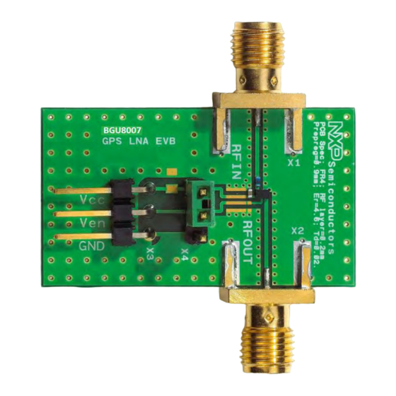
Page 5: Application Circuit
UM10497 NXP Semiconductors BGU8007 GPS LNA EVB 3.1 Application Circuit The circuit diagram of the evaluation board is shown in Fig 2. With jumper JU1 the enable pin can be controlled to either to V or GND. Fig 2. Circuit diagram of the BGU8007 evaluation board 3.2 Board Layout... -
Page 6: Pcb Layout
20um Cu Fig 4. Stack of the PCB material Material supplier is ISOLA DURAVER; r = 4.6 - 4.9: Tan= 0.02 3.4 Bill of materials Table 1 BOM of the BGU8007 GPS LNA EVB v2.1 Designator Description Footprint Value Supplier Name/type... -
Page 7: Required Equipment
UM10497 NXP Semiconductors BGU8007 GPS LNA EVB 4. Required Equipment In order to measure the evaluation board the following is necessary: DC Power Supply up to 30 mA at 1.5 V to 2.2 V; Two RF signal generators capable of generating an RF signal at the operating ... - Page 8 UM10497 NXP Semiconductors BGU8007 GPS LNA EVB 9. For noise under jamming conditions, the following is needed. A 5dB ENR noise source, a directional coupler, GPS band pass filter, a noise-figure analyzer or a spectrum analyzer with noise option can be used. See Fig 11 Fig 5.
-
Page 9: Linearity
UM10497 NXP Semiconductors BGU8007 GPS LNA EVB 6. Linearity At the average power levels of –130 dBm that have to be received by a GPS receiver, the system will not have in-band intermodulation problems caused by the GPS-signal itself. Strong out-of-band cell phone TX jammers however can cause linearity problems, and result in third-order intermodulation products in the GPS frequency band. - Page 10 UM10497 NXP Semiconductors BGU8007 GPS LNA EVB The gain of the DUT was measured between port RFin and RFout of the EVB at the GPS frequency 1575 MHz, while simultaneously a jammer power signal was swept at the 20 dB attenuated input port of the Directional Coupler. Please note that the drive power of the jammer is 20 dB lower at the input of the DUT caused by the directional coupler.
-
Page 11: Noise Figure As Function Of Jammer Power At 850 Mhz And 1850 Mhz
UM10497 NXP Semiconductors BGU8007 GPS LNA EVB (Pin 1575 MHZ = -45 dBm) (Pin 1575 MHZ = -45 dBm) Fig 9. Icc versus jammer power at 1850 MHz Fig 10. Gain versus jammer power at 1850 MHz 7. Noise figure as function of jammer power at 850 MHz and 1850 MHz Noise figure under jamming conditions is a measure of how the LNA behaves when e.g. - Page 12 UM10497 NXP Semiconductors BGU8007 GPS LNA EVB Fig 11. Noise under jamming measurement setup UM10497 All information provided in this document is subject to legal disclaimers. © NXP B.V. 2011. All rights reserved. User manual Rev. 1.0 — 5 October 2011 12 of 16 Arrow.com.
- Page 13 UM10497 NXP Semiconductors BGU8007 GPS LNA EVB In the figures below the noise figure (NF) as function of jammer power are given for 850 MHz and 1850 MHz jammer signals. Fig 12. NF at 1.575 GHz versus jammer power at 850 Fig 13.
-
Page 14: Typical Evaluation Board Results
UM10497 NXP Semiconductors BGU8007 GPS LNA EVB 8. Typical Evaluation Board results Table 2, typical results measured on the Evaluation Boards. Operating Frequency is f=1575.42 MHz unless otherwise specified; Temp = 25 C. Parameter Symbol BGU8007 Unit Remarks Supply Voltage... -
Page 15: Legal Information
Export might require a prior authorization from competent authorities. In no event shall NXP Semiconductors be liable for any indirect, incidental, punitive, special or consequential damages (including - without limitation - Evaluation products — This product is provided on an “as is” and “with all lost profits, lost savings, business interruption, costs related to the removal faults”... -
Page 16: Table Of Contents
UM10497 NXP Semiconductors BGU8007 GPS LNA EVB 10. Contents Introduction ............3 General description ..........4 Application Board ..........4 Application Circuit ..........5 Board Layout ............5 PCB layout ............6 Bill of materials ........... 6 3.4.1 Series inductor ........... 6 Required Equipment ...........
Need help?
Do you have a question about the BGU8007 GPS LNA EVB and is the answer not in the manual?
Questions and answers