
Related Manuals for NXP Semiconductors MPC5748G Low Cost EVB


Summary of Contents for NXP Semiconductors MPC5748G Low Cost EVB
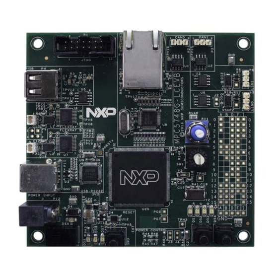
- Page 1 NXP Semiconductors Document Number: MPC5748GLCEVBUG User Guide Rev. 1, 08/2016 MPC5748G Low Cost EVB User Guide (MPC5748G-LCEVB) © 2016 NXP B.V.
-
Page 2: Table Of Contents
User LED’s (DS1, DS2, DS3, DS4) ..........................16 6.5. ADC Input Potentiometer (RVAR, RV1) ........................16 MCU Port Pin LCEVB Functions ............................17 Appendix ................................... 18 Revision History ................................. 34 MPC5748G Low Cost EVB User Guide, Rev. 1, 08/2016 NXP Semiconductors... -
Page 3: Introduction
Ethernet PHY and RJ45 socket (configured for MII mode). USB Type A Host interface. 2 x FlexRay interfaces with standard 2-pin connectors. 14-pin JTAG connector. MPC5748G Low Cost EVB User Guide, Rev. 1, 08/2016 NXP Semiconductors... -
Page 4: Differences To The Customer Evb
Highly configurable via jumper shunts Fixed (limited configuration via 0 ohm resistors) * Daughter card crystals are typically 40 MHz for FXOSC and 32.768 KHz for SXOSC but may vary between daughter cards. MPC5748G Low Cost EVB User Guide, Rev. 1, 08/2016 NXP Semiconductors... - Page 5 LCEVB Features The figure below shows the customer EVB (left) next to the LCEVB (right). Figure 1. Customer and LCEVB side by side MPC5748G Low Cost EVB User Guide, User Guide, Rev. 1, 08/2016 NXP Semiconductors...
-
Page 6: Configuration Overview
Modifications should only be attempted by appropriately trained personnel using the correct equipment and Personal Protective Apparel The diagram below gives an overview of the functional blocks of the LCEVB Figure 2. EVB Functional Blocks MPC5748G Low Cost EVB User Guide, Rev. 1, 08/2016 NXP Semiconductors... -
Page 7: Initial Setup
Moving the slide switch to the right (away from the power connector) will turn the EVB ON. Moving the slide switch to the left (towards the power connector) will turn the EVB OFF. MPC5748G Low Cost EVB User Guide, User Guide, Rev. 1, 08/2016 NXP Semiconductors... -
Page 8: Power Status Led
OR’d together using an AND gate and then connected to the buffer to provide an open-drain output. The “reset-out” circuitry provides a buffered reset signal that can be used to drive any circuitry requiring a reset control from the MCU. MPC5748G Low Cost EVB User Guide, Rev. 1, 08/2016 NXP Semiconductors... -
Page 9: Reset Leds
External reset issued from switch or debug BUT not being issued to MCU (check R137 has not been removed) External reset issued from reset switch or debug and has been issued to MCU. MPC5748G Low Cost EVB User Guide, User Guide, Rev. 1, 08/2016 NXP Semiconductors... -
Page 10: Mcu Clock Configuration
STANDBY exit without any additional code (at the sacrifice of slightly higher STANDBY current), however this can be changed to a pullup if required by removing R147 and fitting the resistor on R56. MPC5748G Low Cost EVB User Guide, Rev. 1, 08/2016 NXP Semiconductors... -
Page 11: Communications & Memory Interfaces
For flexibility, the CAN transceiver I/O is connected to a 0.1” header (P2 for CAN0 / P3 for CAN1) rather than using non-standard DB9 connectors. The pinout of these headers is shown below. Figure 5. CAN Physical Interface Connectors MPC5748G Low Cost EVB User Guide, User Guide, Rev. 1, 08/2016 NXP Semiconductors... -
Page 12: Lin Interfaces (P6, P7)
The LCEVB includes a Type A (Host) USB interface, routed to a USB type A female connector. The USB circuit contains a USB83340 transceiver with a MIC2026-1YM USB power switch. There is no hardware user configuration required to use the USB circuit. MPC5748G Low Cost EVB User Guide, Rev. 1, 08/2016 NXP Semiconductors... -
Page 13: Ethernet Interface (P5)
Note that the LCEVB is supplied with a 40 MHz crystal by default. If FlexRay is configured to use the external clock source, then the crystal should be left at 40 MHz MPC5748G Low Cost EVB User Guide, User Guide, Rev. 1, 08/2016 NXP Semiconductors... -
Page 14: User Interface (I/O)
PD0, PD1, PD2, PD3 – HEX Encoder Switch PA1, PA2 – User pushbutton Switches If you require access to all of the available GPIO pads, the customer EVB and daughter card provides this additional functionality. MPC5748G Low Cost EVB User Guide, Rev. 1, 08/2016 NXP Semiconductors... -
Page 15: User Switches (Sw4, Sw5)
Note that POSN 0 will ensure that no voltage is applied to the pads. This allows the pads to be used as normal GPIO (with 10K pulldown) and accessed at the respective pads on the GPIO matrix area. MPC5748G Low Cost EVB User Guide, User Guide, Rev. 1, 08/2016 NXP Semiconductors... -
Page 16: User Led's (Ds1, Ds2, Ds3, Ds4)
Note that this circuit provides a very rough way to evaluate the ADC. There is a small current limiting series resistor network to limit the injection current to around 4.4 mA. MPC5748G Low Cost EVB User Guide, Rev. 1, 08/2016 NXP Semiconductors... -
Page 17: Mcu Port Pin Lcevb Functions
Pin not accessible on LCEVB USB1 GPIO USB1 GPIO Ethernet GPIO GPIO GPIO GPIO Shared with user switches Shared with Hex Encoder Switch Shared with user LED’s MPC5748G Low Cost EVB User Guide, User Guide, Rev. 1, 08/2016 NXP Semiconductors... -
Page 18: Appendix
8. Appendix The MPC5748G LCEVB schematics, Rev B are shown below. MPC5748G Low Cost EVB User Guide, Rev. 1, 08/2016 NXP Semiconductors... - Page 19 This document contains information proprietary to NXP and shall not be used for engineering design, - All test points (SMT wire loop style) are denoted TPx without the express written permission of NXP Semiconductors. - Test point Vias (just through hole pads) are denoted TPVx...
- Page 20 Power Input and Linear Voltage Regulators Power Supply Input Power Control Jumpers can be fitted to (Power Switch) facilitate power measurements 2.1mm Barrel 5V0_SR 3V3_SR Connector Main Power In 5V-IN MCU_3V3 (SR = Swithing Reg) MCU_3V3 HDR 1X2 0.1UF B340A 10UF R142 5V0_SR...
- Page 21 Calypso MCU Power Connections Power Supply Contraints: Default Configuration: - If VDD_HV_A is driven from 3.3V, VDD_HV_FLA must - ALL MCU supply voltages are set to 3.3V also be supplied from 3.3V (ADC0, ADC1, VDD_HV_A, VDD_HV_B, VDD_HV_C, - If VDD_HV_A is driven from 5V, the VDD_HV_FLA pin VBallast) must be disconnected from 3.3V - VDD_HV_FLA = External 3.3V supplied (jumper...
- Page 22 Calypso MCU Decoupling and bulk storage Flash Capacitor Types: ADC0_CAP ADC1_CAP ADC1REF_CAP HVFLA_CAP 4700pF - Ceramic X7R, 50V 10% 0402 0.1uF - Ceramic X7R, 16V 10% 0402 (Kemet C0402C104K4RAC) 0.68uF - Ceramic X7R, 16V 10% 0805 (Murata GCM219R71C684KA37) C118 0.1UF 0.1UF 2.2UF - Ceramic X7R, 10V...
- Page 23 Reset and External Clock In Reset is in the Reset Input / Output PER_HVA PORST VDD_HVA domain. Connect an external LVI to pad PER_HVA when supplying external 1.25V so that PORST is asserted until exterbal 1.25V supply is at 3V3_SR 10.0K threshold and stable TPH1...
- Page 24 Clocks Oscillators 12PF (EXTAL32) 1.0M 32.768KHZ FC-255 32.7680K-A3 (Load Capacitance 7pF) 12PF (XTAL32) 12PF MCU-EXTAL MCU-EXTAL 1.0M NX8045GB-40.000M-STD-CSJ-1 XTAL 40.0MHZ (Optimised for Automotive, 8pF Load capacitance) 12PF MCU-XTAL MCU-XTAL Automotive Microcontroller Applications East Kilbride, Scotland NXP General Business Use Drawing Title: MPC5748G-LCEVB Page Title: Clocks...
- Page 25 Calypso GPIO 1 of 2 U20A (GPIO) Calypso 176QFP (SW1 & GPIO**) (WKPU2 / NMI0) 14,15 (WKPU3) 14,15 (SW2 & GPIO) (FR_A_TX_EN) (MII_RXCLK) (FR_A_RX) (GPIO) Package 1of3 GPIO Pins1 (FR_B_TX) Key to text colours: (GPIO) (FR_B_RX) Purple - Comms Physical Interfaces (GPIO) Orange - Other Peripherals and I/O (MII_RXD2)
- Page 26 Calypso GPIO 2 of 2 U20C Key to text colours: (GPIO) Calypso 176QFP Purple - Comms Physical Interfaces (GPIO) Orange - Other Peripherals and I/O (GPIO) Blue - Debug (JTAG & Nexus) (GPIO) Package 3of3 GPIO Pins2 Black - Clock, Reset and Control (USB1_STP) - I/O Matrix and other functions (eg LED) (USB1_NXT)
- Page 27 CAN & LIN Physical CAN0 Physical Interface 5V0_SR PER_HVA - 5.0V input supply for CAN transceiver (4.5 to 5.5V) VI/O - determines the signal level on MCU TX and RX pins 0.1UF 0.1UF and can range from 2.8 to 5.5V 2.2UF 2.2UF (0603...
- Page 28 USB RS232 (serial) Interface All Signals are in FTDI USB <-> Serial Interface power domain - Self Powered mode. No power is taken from USB VDD_HV_A. - Device efaults to Dual serial (RS232) mode i.e. RS232 on both A and FTDI interface will work at 3.3V or 5.0V - Configurable I/O voltage on CHA / CHB via VDDIOA/B...
- Page 29 USB (Type A Host and Type AB OTG) General Layout Note. Recommendation is to keep all 3V3_SR 5V0_SR USB Signals are in tracks between MCU and USB PHI less than 3" See power Adobe Acrobat Document additional SMSC Layout guidelines PDF to the right domain 10UF 0.1UF...
- Page 30 Ethernet (Configured for MII Mode) All Ethernet Signals are in power domain VDD_HV_B The Ethernet interface only supports 3V3_SR 3V3_SR 120OHM 3.3V operation. All I/O signals must be 3.3V. If VDD_HVA is set to 5V, Layout Note - Place Caps Ethernet MCU pads must be left as and Resistors close to PHI tri-state...
- Page 31 FlexRAY Physical Interface All Signals are in Decoupling Caps for BOTH IC's. Place next to power pins. Note on VBAT: power domain VDD_HV_A. - Operational range is 6.5v to 60V - Undervoltage detection is max 4.5v FRBATA FRBATB 5V0_SR PER_HVA FlexRAY FlexRAY interface will debug...
- Page 32 User Peripheralls (Led's, Switches and ADC Pot) Switches are hard wired to 3.3V rather than 5V so it's not possible to drive 5V into a 3.3V pad (which would cause damage) Similarly, the LED's are active low with 3.3v supply so can be safely coupled to pads on either 3.3V or 5V domains The ADC input is limited to 3.3V, again to prevent driving 5V into a 3.3V pad which would cause damage User LED's (Active Low) ADC Input Pot and Test Point...
- Page 33 GPIO Pin Matrix All pads are DNP (Do Not Populate) 0.1" pitch headers placed on a 0.1" grid 7,14 PA[1,2] shared with PORTA PORTB PORTD PortF PortI 7,14 user switches PA12 IOM1 IOM5 IOM10 IOM15 PA12 PA13 PA13 PA14 IOM2 IOM6 IOM11 IOM16...
-
Page 34: Revision History
9. Revision History Date Substantial changes March 2016 Initial release August 2016 Rev. 1: Updated Schematics and Board Pictures MPC5748G Low Cost EVB User Guide, Rev. 1, 08/2016 NXP Semiconductors... - Page 35 Information in this document is provided solely to enable system and software How to Reach Us: implementers to use NXP products. There are no express or implied copyright licenses granted hereunder to design or fabricate any integrated circuits based Home Page: on the information in this document.
- Page 36 Mouser Electronics Authorized Distributor Click to View Pricing, Inventory, Delivery & Lifecycle Information: MPC5748G-LCEVB...
Need help?
Do you have a question about the MPC5748G Low Cost EVB and is the answer not in the manual?
Questions and answers