Advertisement
Quick Links
NB3x6x1xxG16QFNEVK
NB3x6x1xxG16QFN
OmniClock Evaluation
Kit Manual
Devices Supported
•
NB3H63143G (QFN16, 3.3V)
•
NB3V63143G (QFN16, 1.8V)
•
NB3H73113G (QFN16, 3.3V)
Introduction
NB3x6x1xxG16QFNEVK is an evaluation kit offering a
convenient solution for evaluating QFN16 devices.
Included are one main board, a daughter board, and a USB
cable. The main board and daughter board are 4 layer boards
with dedicated power and GND planes.
The daughter board plugs directly on to the main board
using four 4−pin header connectors. These connectors route
the signal, power and ground to the device on the daughter
board. The two boards correctly plug into one another in
only one orientation ensuring proper pin alignment. The
daughter board has a 16QFN socket to test NB3x6x1xxG
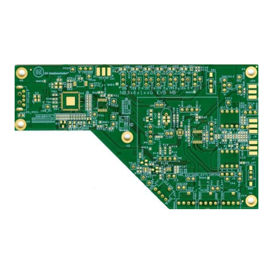
and NB3H73113G devices. A view of the main board with
the 16QFN daughter board is shown in Figures 1 and 2.
The
Clock Cruiser Software is the GUI software
developed to be used with this evaluation kit, and can be
downloaded for free from www.onsemi.com. It allows the
user to set programmable parameters and generate solutions
that fit application needs. These solutions can then be
programmed in to device's OTP memory or be temporarily
written into device registers for evaluation. For more
information on using the GUI, refer to Clock Cruiser User
Guide.
Figure 1. 455 View of Main Board with QFN16
© Semiconductor Components Industries, LLC, 2017
March, 2017 − Rev. 3
Arrow.com.
Downloaded from
Daughter Board
www.onsemi.com
EVAL BOARD USER'S MANUAL
Part Description
The
NB3x6x1xxG and NB3H73113G, which are
members of the OmniClock family, are versatile user
programmable clock
Semiconductor with customer experience in mind. These
devices are tailored to fit into an extensive array of
applications including wearable technology, smart phones,
digital cameras, E−books, portable electronics, and Internet
of Things. The NB3H designated parts are powered by 3.3V
and 2.5V supplies while NB3V parts support 1.8V
operation.
These devices are One Time Programmable (OTP), low
power PLL based clock generators that accept fundamental
mode parallel resonant crystals of up to 50 MHz or a single
ended LVCMOS/LVTTL reference clock input of up to
200 MHz. The outputs can be configured as either three
single ended LVCMOS/LVTTL outputs or a combination of
one
single
ended
output
LVPECL/LVDS/HCSL/CML output. The generated clock
output's frequency can range between 8 kHz to 200 MHz.
Other programmable parameters include internal crystal
load capacitor, drive strength for LVCMOS outputs, output
frequency modulation controls (type, depth, modulation
rate), output phase inversion, and PLL bypass mode. The
devices are fully functional between −40°C to +85°C.
Figure 2. Top View of Main Board with QFN16
Daughter Board
1
generators
designed
by
and
one
differential
Publication Order Number:
EVBUM2308/D
ON
Advertisement

Related Manuals for ON Semiconductor NB3H63143G


Summary of Contents for ON Semiconductor NB3H63143G
- Page 1 NB3x6x1xxG16QFNEVK NB3x6x1xxG16QFN OmniClock Evaluation Kit Manual www.onsemi.com Devices Supported EVAL BOARD USER’S MANUAL • NB3H63143G (QFN16, 3.3V) • NB3V63143G (QFN16, 1.8V) • NB3H73113G (QFN16, 3.3V) Part Description NB3x6x1xxG and NB3H73113G, which are Introduction members of the OmniClock family, are versatile user...
- Page 2 NB3x6x1xxG16QFNEVK Figure 3. Main Board Figure 4. 16QFN Daughter Board www.onsemi.com Arrow.com. Arrow.com. Downloaded from Downloaded from...
-
Page 3: Step 1: Hardware Setup
Slide switches to the position referenced in table below: (ON position is indicated via lettering on switch) Switch No Position 3. Ensure that Crystal (XTAL) is in holder. 4. Place NB3H63143G or NB3V63143G in DUT socket U2. For device pin 1 alignment refer to Figure 4. www.onsemi.com Arrow.com. Arrow.com. -
Page 4: Step 2: Device Programming
NB3x6x1xxG16QFNEVK Step 2: Device Programming Note: Skip this section if device has already been programmed 1. Download and install Clock Cruiser GUI Software to a computer that meets or exceeds minimum requirements found on Clock Cruiser User guide. 2. Connect the evaluation kit to an USB port using included USB cable. A LED next to the USB connector will glow red, indicating that +5 V supply has been applied to EVB. - Page 5 NB3x6x1xxG16QFNEVK Select Output Termination DUT outputs are routed to three SMA connectors on the main board (J7, J9, and J23) to provide termination for CLK0, CLK1, and CLK2 respectively. By turning rotary switches U15 and U16, the board will automatically terminate the programmed output level for CLK0 and CLK1, to its respective output termination in table below.
- Page 6 NB3x6x1xxG16QFNEVK SEL: Pin is used to select between the available four output configurations that can be stored in devices OTP memory. Main board: SEL0=J27, SEL1=J26 Daughter board: SEL0=J30, SEL1=J31 SEL1 Output Configuration SEL0 For NB3x73113G devices, SEL is replaced with SCLK and SDATA signals for I2C / SMBus communication. These devices support one configuration, which can be modified, by writing device registers with a new configuration file created from the Clock Cruiser Software, a freely down loadable GUI software available on www.onsemi.com.
- Page 7 NB3x6x1xxG16QFNEVK APPENDIX Unpopulated Boards Figure 5. Main Board Top View Figure 7. QFN16 Daughter Board Top View Figure 6. Main Board Bottom View Figure 8. QFN16 Daughter Board Bottom View www.onsemi.com Arrow.com. Arrow.com. Arrow.com. Arrow.com. Arrow.com. Arrow.com. Arrow.com. Downloaded from Downloaded from Downloaded from Downloaded from...
-
Page 8: Output Termination
NB3x6x1xxG16QFNEVK OUTPUT TERMINATION HCSL LVPECL LVDS www.onsemi.com Arrow.com. Arrow.com. Arrow.com. Arrow.com. Arrow.com. Arrow.com. Arrow.com. Arrow.com. Downloaded from Downloaded from Downloaded from Downloaded from Downloaded from Downloaded from Downloaded from Downloaded from... - Page 9 NB3x6x1xxG16QFNEVK Main Board Schematic Figure 9. Main Board Schematic (1 of 3) www.onsemi.com Arrow.com. Arrow.com. Arrow.com. Arrow.com. Arrow.com. Arrow.com. Arrow.com. Arrow.com. Arrow.com. Downloaded from Downloaded from Downloaded from Downloaded from Downloaded from Downloaded from Downloaded from Downloaded from Downloaded from...
- Page 10 NB3x6x1xxG16QFNEVK Figure 10. Main Board Schematic (2 of 3) www.onsemi.com Arrow.com. Arrow.com. Arrow.com. Arrow.com. Arrow.com. Arrow.com. Arrow.com. Arrow.com. Arrow.com. Arrow.com. Downloaded from Downloaded from Downloaded from Downloaded from Downloaded from Downloaded from Downloaded from Downloaded from Downloaded from Downloaded from...
- Page 11 NB3x6x1xxG16QFNEVK Figure 11. Main Board Schematic (3 of 3) www.onsemi.com Arrow.com. Arrow.com. Arrow.com. Arrow.com. Arrow.com. Arrow.com. Arrow.com. Arrow.com. Arrow.com. Arrow.com. Arrow.com. Downloaded from Downloaded from Downloaded from Downloaded from Downloaded from Downloaded from Downloaded from Downloaded from Downloaded from Downloaded from Downloaded from...
- Page 12 NB3x6x1xxG16QFNEVK 16QFN Daughter Board Schematic Figure 12. 16QFN Daughter Board Schematic www.onsemi.com Arrow.com. Arrow.com. Arrow.com. Arrow.com. Arrow.com. Arrow.com. Arrow.com. Arrow.com. Arrow.com. Arrow.com. Arrow.com. Arrow.com. Downloaded from Downloaded from Downloaded from Downloaded from Downloaded from Downloaded from Downloaded from Downloaded from Downloaded from Downloaded from Downloaded from...
- Page 13 NB3x6x1xxG16QFNEVK BILL OF MATERIAL MAIN BOARD Notes / Manufac- Manufac- Reference Part Footprint Vendor Vendor PN turer turer Part# Description marks C2,C3 R0402 DigiKey 541−0.0JCT− Vishay Dale RES SMD 0.0 OHM 0.01 mF _Mount R0E CW0402000 JUMPER 1/16W 0Z0ED C8,C31, 22 mF C0603 DigiKey...
- Page 14 NB3x6x1xxG16QFNEVK BILL OF MATERIAL MAIN BOARD Notes / Manufac- Manufac- Reference Part Footprint Vendor Vendor PN turer turer Part# Description marks J15,J16, SMDHeader berg_1x2_ DigiKey 3M5350−ND 151204−232 CONN 4POS 2MM J20,J33, 2−pin 2p54 0−RB HEADER DL STR J34,J35, J36,J37 Conn, USB− USB_A_- DigiKey WM17117−ND...
- Page 15 NB3x6x1xxG16QFNEVK BILL OF MATERIAL MAIN BOARD Notes / Manufac- Manufac- Reference Part Footprint Vendor Vendor PN turer turer Part# Description marks R22,R41, R0402 DigiKey P10KJCT−ND Panasonic ERJ−2GEJ1 RES SMD 10K OHM R54,R55, 5% 1/10W 0402 R56,R58, R61,R65, R67,R68, R69,R70, R71,R72, R74,R76, R78,R79, R80,R81,...
- Page 16 NB3x6x1xxG16QFNEVK BILL OF MATERIAL MAIN BOARD Notes / Manufac- Manufac- Reference Part Footprint Vendor Vendor PN turer turer Part# Description marks U11,U12, S−2151 DigiKey 563−1088−ND Copal S−2151 SW ROTARY DIP U13,U14 Electronics SP4T SIDE KNOB U15,U16 SS−10−15S- DigiKey 563−1078−ND Copal SS−10−15S- SWITCH ROTARY P−LE...
- Page 17 NB3x6x1xxG16QFNEVK BILL OF MATERIAL DAUGHTER BOARD Reference Part PCB Footprint Vendor Vendor PN Manufacturer C13, C15, C17, C19 4.7 mF C0603 DigiKey 587−1782−1−ND Taiyo Yuden C23, C25 R0603 DigiKey 541−0.0GCT−ND Vishay Dale C14, C16, C18, C20 10 mF C0603 DigiKey 587−3383−1−ND Taiyo Yuden VDDO1, VDDO2,...
- Page 18 onsemi, , and other names, marks, and brands are registered and/or common law trademarks of Semiconductor Components Industries, LLC dba “onsemi” or its affiliates and/or subsidiaries in the United States and/or other countries. onsemi owns the rights to a number of patents, trademarks, copyrights, trade secrets, and other intellectual property. A listing of onsemi’s product/patent coverage may be accessed at www.onsemi.com/site/pdf/Patent−Marking.pdf.
Need help?
Do you have a question about the NB3H63143G and is the answer not in the manual?
Questions and answers