Advertisement
Quick Links
NB4N855SMEVB
Evaluation Board User's
Manual for NB4N855S
Description
ON Semiconductor has developed an evaluation board for
the NB4N855S device as a convenience for the customers
interested in performing their own device engineering
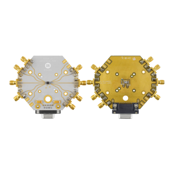
assessment. This board provides a high bandwidth 50 W
controlled impedance environment. The pictures in Figure 1
show the top and bottom view of the evaluation board, which
can be configured in several different ways.
This NB4N855S evaluation board manual contains:
•
Appropriate Lab Setup
•
Assembly Instructions
•
Bill of Materials
This manual should be used in conjunction with the
NB4N855S device data sheet, which contains full technical
details on the device specifications and operation.
Top View
Figure 1. Top and Bottom View of the NB4N855S Evaluation Board
© Semiconductor Components Industries, LLC, 2012
February, 2012 − Rev. 2
EVAL BOARD USER'S MANUAL
Board Lay−Up
The NB4N855S evaluation board is implemented in four
layers with split (dual) power supplies (Figure 6, Evaluation
Board Lay−up). For standard lab setup, a split (dual) power
supply is essential to enable the 50 W internal impedance in
the oscilloscope as a devices termination. The first layer or
primary trace layer is 0.005" thick Rogers RO4003 material,
which is designed to have equal electrical length on all signal
traces from the device under the test (DUT) to the sense
output. The second layer is the 1.0 oz copper ground plane.
The FR4 dielectric material is placed between second and
third layer and between third and fourth layer. The third
layer is also 1.0 oz copper ground plane. The fourth layer is
the secondary trace layer.
Bottom View
1
http://onsemi.com
Publication Order Number:
EVBUM2079/D
Advertisement

Related Manuals for ON Semiconductor NB4N855SMEVB


Summary of Contents for ON Semiconductor NB4N855SMEVB
- Page 1 EVAL BOARD USER’S MANUAL Description Board Lay−Up ON Semiconductor has developed an evaluation board for The NB4N855S evaluation board is implemented in four the NB4N855S device as a convenience for the customers layers with split (dual) power supplies (Figure 6, Evaluation interested in performing their own device engineering Board Lay−up).
- Page 2 NB4N855SMEVB Figure 2. Evaluation Board Lay−up Connecting Power and Ground Planes The side launch 9 pin power supply connector is wired as the PCB to accommodated easier connections. Exact values shown in Figure 3. Test points can be soldered on the top of that need to be applied can be found in Table 1.
- Page 3 Board Components Configuration For the LVDS configuration Input pin pads of the D0 or The NB4N855SMEVB evaluation board requires eight D1 input has to be shorted using 100 W resistor across side SMA connectors. Placement locations are described in differential lines.
- Page 4 NB4N855SMEVB Z = 50 W Z = 50 W OUT1 Z = 50 W OSCILLOSCOPE PIN 1 OUT2 (50 W Scope Head) Z = 50 W SIGNAL GENERATOR Z = 50 W OUT3 Z = 50 W Z = 50 W...
- Page 5 NB4N855SMEVB Table 3. Bill of Materials Components Manufacturer Description Part Number Qty. Web Site Johnson* SMA Connector − Side 142−0701−851 http://www.johnsoncomponents.com Connector Launch 9 Pin D−Sub Amphenol Connector, Female, 788796−1 http://www.amphenol.com Receptacle 9−Pin, Right Angle Surface Mount Keystone* http://www.keyelco.com SMT Miniature Test...
-
Page 6: Package Dimensions
SOLDERING FOOTPRINT* 1.04 0.32 0.041 0.0126 3.20 4.24 5.28 0.126 0.167 0.208 0.50 SCALE 8:1 0.0196 inches *For additional information on our Pb−Free strategy and soldering details, please download the ON Semiconductor Soldering and Mounting Techniques Reference Manual, SOLDERRM/D. http://onsemi.com... - Page 7 onsemi, , and other names, marks, and brands are registered and/or common law trademarks of Semiconductor Components Industries, LLC dba “onsemi” or its affiliates and/or subsidiaries in the United States and/or other countries. onsemi owns the rights to a number of patents, trademarks, copyrights, trade secrets, and other intellectual property. A listing of onsemi’s product/patent coverage may be accessed at www.onsemi.com/site/pdf/Patent−Marking.pdf.
- Page 8 Mouser Electronics Authorized Distributor Click to View Pricing, Inventory, Delivery & Lifecycle Information: onsemi NB4N855SMEVB...
Need help?
Do you have a question about the NB4N855SMEVB and is the answer not in the manual?
Questions and answers