Advertisement
Quick Links
NB7L14MNGEVB
NB7L14MNG
Evaluation Board
User's Manual
Introduction
ON Semiconductor has developed the QFN16EVB
evaluation board for its high-performance devices packaged
in the 16-pin QFN. This evaluation board was designed to
provide a flexible and convenient platform to quickly
evaluate, characterize and verify the operation of various
ON Semiconductor products. Many QFN16EVBs are
dedicated with a device already installed, and can be ordered
from www.onsemi.com at the specific device web page.
This evaluation board manual contains:
•
Information on 16-lead QFN Evaluation Board
•
Assembly Instructions
•
Appropriate Lab Setup
•
Bill of Materials
This user's manual provides detailed information on
board contents, layout and its use. It should be used in
conjunction with an appropriate ON Semiconductor device
datasheet located at www.onsemi.com. The datasheet
contains the technical device specifications.
© Semiconductor Components Industries, LLC, 2013
May, 2013 − Rev. 0
Arrow.com.
Downloaded from
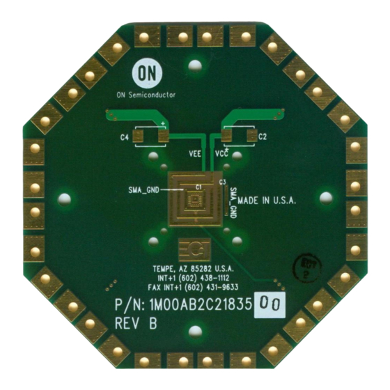
Top View
Figure 1. Top and Bottom View of the 16 QFN Evaluation Board
http://onsemi.com
EVAL BOARD USER'S MANUAL
Board Layout
The QFN16 Evaluation Board provides a high bandwidth,
50 W
controlled
impedance
implemented in four layers. The first layer or primary trace
layer is 0.008" thick Rogers RO4003 material, and is
designed to have equal electrical length on all signal traces
from the device under test (DUT) pins to the SMA
connectors. The second layer is the 1.0 oz copper ground
plane and is primarily dedicated for the SMA connector
ground plane. FR4 dielectric material is placed between the
second and third layers and between third and fourth layers.
The third layer is also 1.0 oz copper plane. A portion of this
layer is designated for the device V
planes. The fourth layer is the secondary trace layer.
Bottom View
1
environment
and
is
and DUTGND power
CC
Publication Order Number:
EVBUM2184/D
Advertisement

Related Manuals for ON Semiconductor NB7L14MNGEVB


Summary of Contents for ON Semiconductor NB7L14MNGEVB
- Page 1 It should be used in The third layer is also 1.0 oz copper plane. A portion of this conjunction with an appropriate ON Semiconductor device layer is designated for the device V and DUTGND power datasheet located at www.onsemi.com.
-
Page 2: Silkscreen (Top Side)
NB7L14MNGEVB Figure 2. Enlarged Bottom View VEE/DUTGND SMA_GND Pin 12 Pin 1 Pin 11 Pin 2 DUT_GND Pin 10 Pin 3 Pin 9 Pin 4 Figure 3. Enlarged Bottom View of the Evaluation Board SILKSCREEN (TOP SIDE) LAYER 1 (TOP SIDE) 1 OZ ROGERS 4003 0.008 in... - Page 3 NB7L14MNGEVB Top View Bottom View Figure 5. Evaluation Board Layout Evaluation Board Assembly Instructions confusion with the use of this board, the negative supply The QFN−16 evaluation board is designed for connector is labeled V /DUTGND. SMAGND is the characterizing devices in a 50 W laboratory environment ground for the SMA connectors and is not to be confused using high bandwidth equipment.
- Page 4 NB7L14MNGEVB CML Outputs Installing the SMA Connectors Likewise, CML outputs need to be terminated to V Each configuration indicates the number of SMA a 50 W resistor. If no internal resistors are provided on the connectors needed to populate an evaluation board for a given device.
- Page 5 NB7L14MNGEVB NB7L14MNGEVB ASSEMBLY Table 1. CONFIGURATION FOR DEVICE: NB7L14 Device Pin # Connector Wire NOTE: DUTGND/V = Exposed Pad and must be tied to DUTGND/V CONFIGURATIONS DUTGND/V Exposed Pad SMAGND Top View VEE/DUTGND Polarity of 22 mF: + C4 −...
- Page 6 NB7L14MNGEVB NB7L14MNGEVB TEST Power Supply /DUTGND Test Measuring Differential Equipment Signal Generator DUTGND/ Channel 1 Channel 2 ExPad SMAGND Trigger Trigger GND (0 V) DUTGND Power Supply 1. Connect appropriate power supplies to V /DUTGND, SMAGND, and ExPad (see Table 2).
- Page 7 NB7L14MNGEVB Table 4. BILL OF MATERIALS Components Manufacturer Description Part Number Web Site SMA Connector Rosenberger SMA Connector, Side 32K243−40ME3 http://www.rosenberger.de Launch, Gold Plated http://www.rosenbergerna.com Surface Mount Keystone* SMT Miniature Test 5015 http://www.keyelco.com Point Test Points Chip Capacitor AVC Corporation* http://www.avxcorp.com...
- Page 8 NB7L14MNGEVB Top Layer Second Layer (SMA_GND Plane) Figure 9. Gerber Files http://onsemi.com Arrow.com. Downloaded from...
- Page 9 NB7L14MNGEVB Third Layer (DUT_GND Trace) Bottom Layer Figure 10. Gerber Files http://onsemi.com Arrow.com. Downloaded from...
-
Page 10: Additional Information
onsemi, , and other names, marks, and brands are registered and/or common law trademarks of Semiconductor Components Industries, LLC dba “onsemi” or its affiliates and/or subsidiaries in the United States and/or other countries. onsemi owns the rights to a number of patents, trademarks, copyrights, trade secrets, and other intellectual property. A listing of onsemi’s product/patent coverage may be accessed at www.onsemi.com/site/pdf/Patent−Marking.pdf.
Need help?
Do you have a question about the NB7L14MNGEVB and is the answer not in the manual?
Questions and answers