Advertisement
Quick Links
NB6L295MNGEVB,
NB6L295MMNGEVB
NB6L295MNG/
NB6L295MMNG Evaluation
Board User's Manual
Introduction and Board Description
The NB6L295M Evaluation Board was designed to
provide a flexible and convenient platform to quickly
evaluate, characterize and verify the operation and
performance of either the NB6L295MMNG (CML) or the
NB6L295MNG (LVPECL) Dual Channel Programmable
Delay.
This evaluation board manual contains:
•
Information on the NB6L295M Evaluation Board
•
Appropriate Lab Setup
•
Detailed Board Features
•
Bill of Materials
This manual should be used in conjunction with the device
datasheet NB6L295M/D or NB6L295/D which contains full
technical details on the device specifications and operation.
The NB6L295M Evaluation Board was also designed to
accommodate a custom QFN−24 socket. Therefore, some
external components were installed on the bottom side of the
board.
Board Features
•
On board programmable SDI circuitry minimizing
cabling, or, external SDI accessed through SMA
connectors.
•
Convenient and compact board layout
•
2.5 V or 3.3 V single or split−power supply operation
(banana jack connectors for VCC, SMAGND and
DUTGND; Separate PLDVCC power supply for on
board PLD
•
CML or LVPECL differential output signals are
accessed via SMA connectors with provision for load
termination resistors
© Semiconductor Components Industries, LLC, 2012
April, 2012− Rev. 3
EVAL BOARD USER'S MANUAL
•
SMA connectors are provided for 1) all high−speed
differential input & (CML or LVPECL) output signals
and 2) for external SDI & control signals access
Board Layout
The evaluation board is constructed in four layers. The top
layer is the primary trace layer and is made with polyimide
material. This layer provides a high−bandwidth 50 W
controlled trace impedance environment for the equal length
inputs and outputs. The second layer is a copper ground
plane.
Layer Stack
L1
Signal − "High and Low Speed"
L2
SMA Ground
L3
VCC (Device positive power supply) and DUTGND
(Device negative power supply)
L4
Signal − "Low Speed"
What measurements can you expect to make?
With this evaluation board, the following measurements
could be performed in single ended or differential modes of
operation.
•
Propagation and Programmed Delay
•
Output Rise and Fall Time
•
Frequency Performance
•
Jitter
•
VCMR − Common Mode Range
1
http://onsemi.com
Publication Order Number:
EVBUM2082/D
Advertisement

Related Manuals for ON Semiconductor NB6L295MNGEVB


Summary of Contents for ON Semiconductor NB6L295MNGEVB
- Page 1 NB6L295MNGEVB, NB6L295MMNGEVB NB6L295MNG/ NB6L295MMNG Evaluation Board User's Manual http://onsemi.com EVAL BOARD USER’S MANUAL Introduction and Board Description • The NB6L295M Evaluation Board was designed to SMA connectors are provided for 1) all high−speed provide a flexible and convenient platform to quickly differential input &...
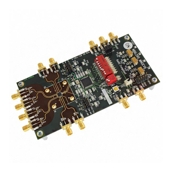
- Page 2 NB6L295MNGEVB, NB6L295MMNGEVB Figure 1. NB6L295MNGEVB Evaluation Board Photo Figure 2. NB6L295MMNGEVB Evaluation Board Photo http://onsemi.com...
- Page 3 NB6L295MNGEVB, NB6L295MMNGEVB DUTGND = PLDGND On−Board SDI Control for 11−Bit Delay Register Push Button to Load Selected Dx External Control Delay Bits Inputs for SDI PLD for SDI Control Data / Clock IN0 Data / Clock IN1 Figure 3. NB6L295M Evaluation Board Layout Overview...
- Page 4 NB6L295MNGEVB, NB6L295MMNGEVB TEST AND MEASUREMENT SETUP AND PROCEDURE Basic Lab Equipment (or Equivalent) Dual Power Supplies • Agilent Signal Generator #8133A for INx / INx, external Clock or Data source • +2.5 V Tektronix TDS8000 Oscilloscope or Frequency Counter −...
- Page 5 NB6L295MNGEVB, NB6L295MMNGEVB Step 2: CML & LVPECL Output Load Termination Step 4: Program the SDI The internal delay registers of the NB6L295/NB6L295M NB6L295M − CML Outputs (see Figures 4 and 7) may be programmed by a) the onboard PLD or b) by using The CML Qx and Qx outputs must be externally DC the three−lines for an external Serial Data Interface (SDI)
- Page 6 NB6L295MNGEVB, NB6L295MMNGEVB SMAGND = 0 V VCC = +2.0 V DUTGND = −0.5 V / −1.3 V PLDVCC = +2.0 V Signal Signal Generator Generator Trigger Trigger Digital Oscilloscope or Frequency Counter 50 W 50 W 50 W 50 W Trigger Figure 6.
- Page 7 NB6L295MNGEVB, NB6L295MMNGEVB SMAGND = 0 V VCC = 0 V DUTGND = −2.5 V / −3.3 V PLDVCC = 0 V Signal Signal Generator Generator Trigger Trigger Digital Oscilloscope or Frequency Counter 50 W 50 W 50 W 50 W...
- Page 8 NB6L295MNGEVB, NB6L295MMNGEVB http://onsemi.com...
- Page 9 NB6L295MNGEVB, NB6L295MMNGEVB http://onsemi.com...
- Page 10 NB6L295MNGEVB, NB6L295MMNGEVB http://onsemi.com...
- Page 11 NB6L295MNGEVB, NB6L295MMNGEVB Table 3. NB6L295MMNGEVB BILL OF MATERIALS Item Qty Part Number Value Ref. Des. PCB Footprint Vendor Vendor PN Manufacturer 22 C0603C103K5RACTU 0.01 mF C1,C2,C3,C4,C7,C8,C9,C10,C11 Digikey 399−1091−1−ND Kemet C12,C13,C15,C17,C18,C20,C22 C23,C24,C25,C26,C27,C29 C0805C105K4RACTU 1 mF C6,C5 Digikey 399−1284−1−ND Kemet T494D226K016AS 22 mF C14,C19,C28 EIA−7343−31...
- Page 12 onsemi, , and other names, marks, and brands are registered and/or common law trademarks of Semiconductor Components Industries, LLC dba “onsemi” or its affiliates and/or subsidiaries in the United States and/or other countries. onsemi owns the rights to a number of patents, trademarks, copyrights, trade secrets, and other intellectual property. A listing of onsemi’s product/patent coverage may be accessed at www.onsemi.com/site/pdf/Patent−Marking.pdf.
Need help?
Do you have a question about the NB6L295MNGEVB and is the answer not in the manual?
Questions and answers