Advertisement
Quick Links
NB3N502DEVB
NB3N502DEVB Evaluation
Board User's Manual
Description
The NB3N502 Evaluation Board was designed to provide
a flexible and convenient platform to quickly evaluate,
characterize and verify the performance and operation of the
NB3N502 PLL Clock Multiplier. This user's manual
provides detailed information on the board's contents,
layout and use, and it should be used in conjunction with the
NB3N502 data sheet which contains full technical details on
device specifications and operation (www.onsemi.com).
Board Features
•
Fully Assembled Evaluation Board
•
Accommodates the Electrical Characterization of the
NB3N502 in the SOIC−8 Package
© Semiconductor Components Industries, LLC, 2012
February, 2012 − Rev. 1
•
Supports the Use of a 5 MHz to 27 MHz Through−hole
or Surface Mount Crystal
•
SMA Connectors are Provided for Auxiliary Input and
Output Interfaces
•
Incorporates Onboard Slide Switch Controlled
Multiplier Select Pins, Minimizing Excess Cabling
This Evaluation Board Manual Contains
•
Information on the NB3N502 Evaluation Board
•
Appropriate Lab Setup
•
Evaluation Board Layout
•
Bill of Materials
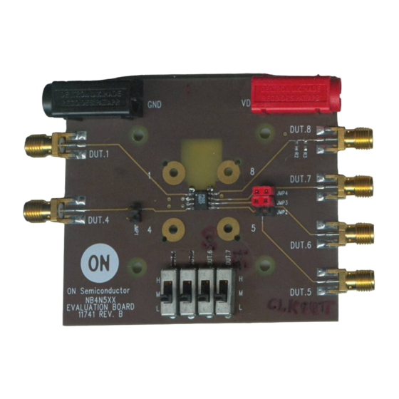
Figure 1. NB3N502 Evaluation Board
1
http://onsemi.com
EVAL BOARD USER'S MANUAL
Publication Order Number:
EVBUM2064/D
Advertisement

Related Manuals for ON Semiconductor NB3N502DEVB


Summary of Contents for ON Semiconductor NB3N502DEVB
- Page 1 NB3N502DEVB NB3N502DEVB Evaluation Board User's Manual http://onsemi.com EVAL BOARD USER’S MANUAL Description • The NB3N502 Evaluation Board was designed to provide Supports the Use of a 5 MHz to 27 MHz Through−hole a flexible and convenient platform to quickly evaluate,...
- Page 2 NB3N502DEVB SETUP FOR MEASUREMENTS Basic Equipment mode crystal should be used. The evaluation board includes • Signal Generator (for External Reference Clock Input) pads for small capacitors from X1/CLK to ground and from X2 to ground. These capacitors, CL1 and CL2, are used to •...
- Page 3 NB3N502DEVB 1. Using the SMA Connectors Table 2. CLOCK MULTIPLIER SELECT TABLE a. SMA connectors J3 and J4 (DUT.6 and DUT.7) S0** should be pulled to V for logic level HIGH, SW4 (DUT.7) SW3 (DUT.6) Multiplier pulled to GND for logic level LOW, and left OPEN for logic level M.
- Page 4 NB3N502DEVB Open Traces (Intentional) For Crystal Use If using the slide switches in- SMA/DUT GND stead of provided SMA con- nectors, short JMP3 and X1/CLK Signal Generator JMP4 (see Table 3). DUT.8 DUT.1 50 W 2 MHz to 50 MHz...
-
Page 5: Board Layout
NB3N502DEVB BOARD LAYOUT The evaluation board is constructed with Getek material with 50 W trace impedances and is designed to minimize noise, achieve high bandwidth and minimize crosstalk. Layer Stack L1 Signal L2 Ground L3 V L4 Signal DUT.8 X1/CLK DUT.1... - Page 6 NB3N502DEVB DUT.8 DUT.1 X1/CLK DUT.7 DUT.4 DUT.6 DUT.5 Figure 8. NB3N502 Evaluation Board Power Layer Figure 9. NB3N502 Evaluation Board Bottom Layer http://onsemi.com...
- Page 7 NB3N502DEVB Figure 10. NB3N502 Evaluation Board Top Assembly Figure 11. NB3N502 Evaluation Board Bottom Assembly http://onsemi.com...
- Page 8 LIMITATIONS OF LIABILITY: ON Semiconductor shall not be liable for any special, consequential, incidental, indirect or punitive damages, including, but not limited to the costs of requalification, delay, loss of profits or goodwill, arising out of or in connection with the board, even if ON Semiconductor is advised of the possibility of such damages. In no event shall ON Semiconductor’s aggregate liability from any obligation arising out of or in connection with the board, under any theory of liability, exceed the purchase price paid for the board, if any.
Need help?
Do you have a question about the NB3N502DEVB and is the answer not in the manual?
Questions and answers