Advertisement
Quick Links
NB3M8T3910GEVB
NB3M8T3910G Evaluation
Board User's Manual
Introduction
The NB3M8T3910GEVB is a custom evaluation board
developed by ON Semiconductor for the NB3M8T3910G.
This evaluation board was designed to provide a flexible and
convenient platform to quickly evaluate, characterize and
verify the operation of the NB3M8T3910G.
This evaluation board manual contains:
•
Information on the NB3M8T3910G Evaluation Board
•
Assembly Instructions
•
Test and Measurement Setup Procedures
•
Bill of Materials
The NB3M8T3910G has two banks of 5 differential
outputs. Each output bank can be independently selected as
LVPECL, LVDS or HCSL outputs by the SMODEAx/Bx
select pins.
This evaluation board, NB3M8T3910GEVB, has been
configured to evaluate each output type.
Of the ten possible differential outputs, three are dedicated
as LVPECL, three are dedicated as LVDS and four are
dedicated as HCSL (labeled on board).
© Semiconductor Components Industries, LLC, 2014
September, 2014 − Rev. 0
Arrow.com.
Downloaded from
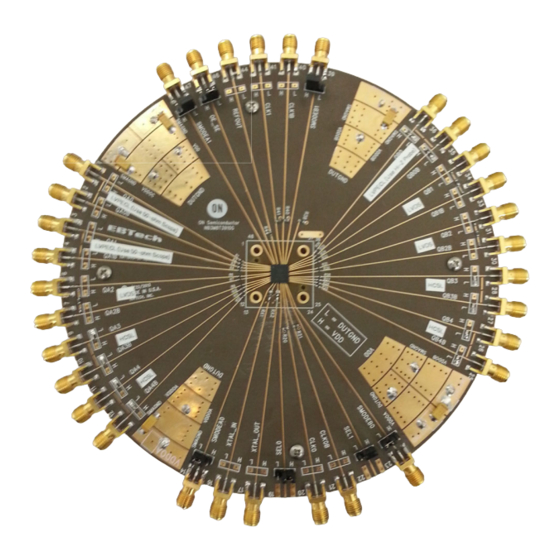
Top View
Figure 1. NB3M8T3910GEVB Top and Bottom View
READ FIRST − INTRODUCTION
http://onsemi.com
EVAL BOARD USER'S MANUAL
This manual should be used in conjunction with the device
datasheet
NB3M8T3910/D
details on the device specifications and operation.
Bottom View
The Single-Ended LVCMOS Output, REFOUT, is
controlled by the Synchronous OE_SE pin. For Clock
frequencies above 250 MHz, the REFOUT line should be
disabled.
Each dedicated output pair on the board is configured per
Table 1 below:
1
which contains full technical
Publication Order Number:
EVBUM2238/D
Advertisement

Related Manuals for ON Semiconductor NB3M8T3910G


Summary of Contents for ON Semiconductor NB3M8T3910G
- Page 1 Bottom View Figure 1. NB3M8T3910GEVB Top and Bottom View READ FIRST − INTRODUCTION The NB3M8T3910G has two banks of 5 differential The Single-Ended LVCMOS Output, REFOUT, is outputs. Each output bank can be independently selected as controlled by the Synchronous OE_SE pin. For Clock...
- Page 2 NB3M8T3910GEVB Table 1. OUTPUT DEDICATION OF THE NB3M8T3910GEVB Output Type (Dedicated) Output Pin Name SMODEA [1:0] SMODEB [1:0] Output Measurement Method QA0/QA0b LVPECL Use 50-W Scope Head; there is no load on the board QA1/QA1b LVPECL Use 50-W Scope Head; there is no load on the board QA2/QA2b LVDS Measure with Single or Differential Hi-Z Probes;...
- Page 3 NB3M8T3910GEVB HCSL OUTPUT CONFIGURATION = 33-W for HCSL Outputs CL = 2 pF Capacitor series to GND for HCSL Outputs Figure 3. HCSL Output Configuration HCSL outputs are typically loaded and terminated with installed for each HCSL output. Also, there is a CL = 2 pF = 33-W and 50-W to ground.
- Page 4 NB3M8T3910GEVB “Split” or Dual Power Supply Connections QUICK START LAB SET-UP USER’S GUIDE Dual Power Supply Power-Up, Input and Output Connections 1. Connect the VDD and VDDOx banana jacks with power supply cables to +3.3 V, and DUTGND +2.0 V +1.3 V and SMAGND to 0 V.
- Page 5 NB3M8T3910GEVB VDDOC VDDOB Signal Generator Oscilloscope OUTb Trigger In Trigger Out SMAGND VDDOA DUTGND Figure 9. Typical Lab Test Set-Up Board Layout second layer is the 0.5 oz copper ground plane and is The custom QFN−48 Evaluation Board provides a high dedicated for the SMA connector ground plane.
- Page 6 NB3M8T3910GEVB SMAGND is the ground for the SMA connectors, is always Power Supply Configuration Install the power supply banana jacks on the bottom side; 0 V and is not to be confused with the device ground, install the appropriate bypass capacitors on top and bottom DUTGND.
- Page 7 NB3M8T3910GEVB LVPECL QA1/QA1b 50-W TO GND OF OSCILLOSCOPE Figure 12. 50 MHz Figure 13. 100 MHz Figure 14. 250 MHz Figure 15. 500 MHz Figure 16. 1000 MHz Figure 17. 1250 MHz http://onsemi.com Arrow.com. Arrow.com. Arrow.com. Arrow.com. Arrow.com. Arrow.com. Arrow.com. Downloaded from Downloaded from Downloaded from...
- Page 8 NB3M8T3910GEVB LVPECL QA1/QA1b 50-W TO GND OF OSCILLOSCOPE Figure 18. 1500 MHz http://onsemi.com Arrow.com. Arrow.com. Arrow.com. Arrow.com. Arrow.com. Arrow.com. Arrow.com. Arrow.com. Downloaded from Downloaded from Downloaded from Downloaded from Downloaded from Downloaded from Downloaded from Downloaded from...
- Page 9 NB3M8T3910GEVB LVPECL QB0/QB0b HI-Z PROBE OSCILLOSCOPE Figure 19. 50 MHz Figure 20. 100 MHz Figure 21. 250 MHz Figure 22. 500 MHz Figure 23. 1000 MHz Figure 24. 1250 MHz http://onsemi.com Arrow.com. Arrow.com. Arrow.com. Arrow.com. Arrow.com. Arrow.com. Arrow.com. Arrow.com. Arrow.com. Downloaded from Downloaded from Downloaded from...
- Page 10 NB3M8T3910GEVB LVPECL QB0/QB0b HI-Z PROBE OSCILLOSCOPE Figure 25. 1500 MHz http://onsemi.com Arrow.com. Arrow.com. Arrow.com. Arrow.com. Arrow.com. Arrow.com. Arrow.com. Arrow.com. Arrow.com. Arrow.com. Downloaded from Downloaded from Downloaded from Downloaded from Downloaded from Downloaded from Downloaded from Downloaded from Downloaded from Downloaded from...
- Page 11 NB3M8T3910GEVB LVDS QB1/QB1b SINGLE-ENDED HI-Z PROBE OSCILLOSCOPE Figure 26. 50 MHz Figure 27. 100 MHz Figure 28. 250 MHz Figure 29. 500 MHz Figure 30. 1000 MHz Figure 31. 1250 MHz http://onsemi.com Arrow.com. Arrow.com. Arrow.com. Arrow.com. Arrow.com. Arrow.com. Arrow.com. Arrow.com. Arrow.com.
- Page 12 NB3M8T3910GEVB LVDS QB1/QB1b SINGLE-ENDED HI-Z PROBE OSCILLOSCOPE Figure 32. 1500 MHz http://onsemi.com Arrow.com. Arrow.com. Arrow.com. Arrow.com. Arrow.com. Arrow.com. Arrow.com. Arrow.com. Arrow.com. Arrow.com. Arrow.com. Arrow.com. Downloaded from Downloaded from Downloaded from Downloaded from Downloaded from Downloaded from Downloaded from Downloaded from Downloaded from Downloaded from Downloaded from...
- Page 13 NB3M8T3910GEVB LVDS QB1/QB1b DIFFERENTIAL HI-Z PROBE OSCILLOSCOPE Figure 33. 50 MHz Figure 34. 100 MHz Figure 35. 250 MHz Figure 36. 500 MHz Figure 37. 1000 MHz Figure 38. 1250 MHz http://onsemi.com Arrow.com. Arrow.com. Arrow.com. Arrow.com. Arrow.com. Arrow.com. Arrow.com. Arrow.com. Arrow.com.
- Page 14 NB3M8T3910GEVB LVDS QB1/QB1b DIFFERENTIAL HI-Z PROBE OSCILLOSCOPE Figure 39. 1500 MHz http://onsemi.com Arrow.com. Arrow.com. Arrow.com. Arrow.com. Arrow.com. Arrow.com. Arrow.com. Arrow.com. Arrow.com. Arrow.com. Arrow.com. Arrow.com. Arrow.com. Arrow.com. Downloaded from Downloaded from Downloaded from Downloaded from Downloaded from Downloaded from Downloaded from Downloaded from Downloaded from Downloaded from...
- Page 15 NB3M8T3910GEVB HCSL QA3/QA3b 50-W TO GND OF OSCILLOSCOPE Figure 40. 50 MHz Figure 41. 100 MHz Figure 42. 250 MHz http://onsemi.com Arrow.com. Arrow.com. Arrow.com. Arrow.com. Arrow.com. Arrow.com. Arrow.com. Arrow.com. Arrow.com. Arrow.com. Arrow.com. Arrow.com. Arrow.com. Arrow.com. Arrow.com. Downloaded from Downloaded from Downloaded from Downloaded from Downloaded from...
- Page 16 NB3M8T3910GEVB HCSL QB3/QB3b HI−Z PROBE OSCILLOSCOPE Figure 43. 50 MHz Figure 44. 100 MHz Figure 45. 250 MHz http://onsemi.com Arrow.com. Arrow.com. Arrow.com. Arrow.com. Arrow.com. Arrow.com. Arrow.com. Arrow.com. Arrow.com. Arrow.com. Arrow.com. Arrow.com. Arrow.com. Arrow.com. Arrow.com. Arrow.com. Downloaded from Downloaded from Downloaded from Downloaded from Downloaded from Downloaded from...
- Page 17 NB3M8T3910GEVB LVCMOS REFOUT Figure 46. 50 MHz Figure 47. 100 MHz Figure 48. 200 MHz http://onsemi.com Arrow.com. Arrow.com. Arrow.com. Arrow.com. Arrow.com. Arrow.com. Arrow.com. Arrow.com. Arrow.com. Arrow.com. Arrow.com. Arrow.com. Arrow.com. Arrow.com. Arrow.com. Arrow.com. Arrow.com. Downloaded from Downloaded from Downloaded from Downloaded from Downloaded from Downloaded from Downloaded from...
-
Page 18: Bill Of Materials
1/4 × 5/8 Screw Screw, 4-40 × 0.25, Building Fasteners PMS 440 0025 PH Digi-Key H342-ND Evaluation Board NB3M8T3910GEVB ON Semiconductor NB3M8T3910GEVB QFN-48 Evaluation Board Device Under Test ON Semiconductor NB3M8T3910G www.onsemi.com NOTE: Components are available through most distributors, i.e. www.newark.com, www.Digikey.com... - Page 19 onsemi, , and other names, marks, and brands are registered and/or common law trademarks of Semiconductor Components Industries, LLC dba “onsemi” or its affiliates and/or subsidiaries in the United States and/or other countries. onsemi owns the rights to a number of patents, trademarks, copyrights, trade secrets, and other intellectual property. A listing of onsemi’s product/patent coverage may be accessed at www.onsemi.com/site/pdf/Patent−Marking.pdf.
Need help?
Do you have a question about the NB3M8T3910G and is the answer not in the manual?
Questions and answers