Table of Contents
Advertisement
Quick Links
www.ti.com
User's Guide
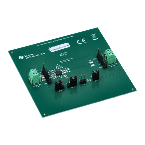
TPSM8286xAA0xEVM Evaluation Module
The TPSM8286xAA0xEVM facilitates the evaluation of the TPSM82864AA0SRDJR and TPSM82866AA0SRDJR
4-A and 6-A pin-to-pin compatible step-down power modules with DCS-Control in a 3.5-mm × 4-mm x 1.4-mm
overmolded QFN package and the TPSM82864AA0HRDMR and TPSM82866AA0HRDMR 4-A and 6-A pin-to-
pin compatible step-down power modules with DCS-Control in a 3.5-mm × 4-mm x 1.8-mm overmolded QFN
package. The EVMs provide a 1.2-V output voltage with 1% accuracy for input voltages from 2.4 V to 5.5 V. The
TPSM82864A and TPSM82866A are high-efficiency and small solutions for the following:
•
Point-of-load (POL) power in applications such as the core supply for FPGAs, CPUs, and ASICs
•
Optical modules
•
Medical imaging
•
Industrial transport
•
Solid state drives (SSDs)
•
Other space-limited applications
1
Introduction.............................................................................................................................................................................2
1.1 Performance Specification.................................................................................................................................................
1.2 Modifications......................................................................................................................................................................
2
Setup........................................................................................................................................................................................4
2.1
Setup..................................................................................................................................................................................4
2.2 Input, Output Connector and Jumper Descriptions............................................................................................................
Instructions..................................................................................................................................................................4
Results.............................................................................................................................................................................5
Layout...........................................................................................................................................................................7
Materials.............................................................................................................................................7
6.1 Schematic..........................................................................................................................................................................
Materials...................................................................................................................................................................9
History......................................................................................................................................................................9
Figure 1-1. Loop Response Measurement Modification..............................................................................................................
Figure 4-1. Thermal Performance (TPSM82866AA0SEVM, V
Figure 4-2. Thermal Performance (TPSM82866AA0HEVM, V
Figure 5-1. Top Assembly............................................................................................................................................................
Layer...................................................................................................................................................................7
Figure 5-3. Internal Layer 1.........................................................................................................................................................
Figure 5-4. Internal Layer 2.........................................................................................................................................................
Figure 5-5. Bottom Layer.............................................................................................................................................................
Figure 5-6. Bottom Layer (Mirrored)............................................................................................................................................
Figure 6-1. TPSM8286xAA0xEVM Schematic............................................................................................................................
Table 6-1. TPSM8286xAA0xEVM Bill of Materials......................................................................................................................
Trademarks
All trademarks are the property of their respective owners.
SLVUCB0A - SEPTEMBER 2021 - REVISED NOVEMBER 2022
Submit Document Feedback
ABSTRACT
Table of Contents
List of Figures
= 5 V, V
= 5 V, V
= 1.2 V, I
IN
OUT
List of Tables
Summary..........................................................................................................................2
Copyright © 2022 Texas Instruments Incorporated
= 6
A)...............................................5
= 6 A)..............................................
= 6 A)........................................................................
OUT
TPSM8286xAA0xEVM Evaluation Module
Table of Contents
2
2
4
8
3
5
6
7
7
7
7
7
8
9
1
Advertisement
Table of Contents

Related Manuals for Texas Instruments TPSM8286 AA0 Series


Summary of Contents for Texas Instruments TPSM8286 AA0 Series
-
Page 1: Table Of Contents
Table 1-1. Performance Specification Summary..........................2 Table 6-1. TPSM8286xAA0xEVM Bill of Materials........................Trademarks All trademarks are the property of their respective owners. SLVUCB0A – SEPTEMBER 2021 – REVISED NOVEMBER 2022 TPSM8286xAA0xEVM Evaluation Module Submit Document Feedback Copyright © 2022 Texas Instruments Incorporated... -
Page 2: Introduction
With these changes, an AC signal (10-mV, peak-to-peak amplitude recommended) can be injected into the control loop across the added 10-Ω resistor. Figure 4-3 shows the results of this test. TPSM8286xAA0xEVM Evaluation Module SLVUCB0A – SEPTEMBER 2021 – REVISED NOVEMBER 2022 Submit Document Feedback Copyright © 2022 Texas Instruments Incorporated... -
Page 3: Figure 1-1. Loop Response Measurement Modification
Introduction Figure 1-1. Loop Response Measurement Modification SLVUCB0A – SEPTEMBER 2021 – REVISED NOVEMBER 2022 TPSM8286xAA0xEVM Evaluation Module Submit Document Feedback Copyright © 2022 Texas Instruments Incorporated... -
Page 4: Setup
High currents may be present on the input and output. Use connectors J1 and J2 if the current exceeds 3 A. TPSM8286xAA0xEVM Evaluation Module SLVUCB0A – SEPTEMBER 2021 – REVISED NOVEMBER 2022 Submit Document Feedback Copyright © 2022 Texas Instruments Incorporated... -
Page 5: Test Results
= 6 A) Figure 4-2. Thermal Performance (TPSM82866AA0HEVM, V = 5 V, V = 1.2 V, I = 6 A) SLVUCB0A – SEPTEMBER 2021 – REVISED NOVEMBER 2022 TPSM8286xAA0xEVM Evaluation Module Submit Document Feedback Copyright © 2022 Texas Instruments Incorporated... -
Page 6: Out = 1.2 V, Iout = 6 A)
1000000 Frequency (Hz) Figure 4-3. Loop Response Measurement (V = 5 V, V = 1.2 V, I = 6 A) TPSM8286xAA0xEVM Evaluation Module SLVUCB0A – SEPTEMBER 2021 – REVISED NOVEMBER 2022 Submit Document Feedback Copyright © 2022 Texas Instruments Incorporated... -
Page 7: Board Layout
Figure 5-6. Bottom Layer (Mirrored) 6 Schematic and Bill of Materials This section provides the TPSM8286xAA0xEVM schematic and bill of materials (BOM). SLVUCB0A – SEPTEMBER 2021 – REVISED NOVEMBER 2022 TPSM8286xAA0xEVM Evaluation Module Submit Document Feedback Copyright © 2022 Texas Instruments Incorporated... -
Page 8: Schematic
PGND PGND PGND PGND PGND PGND PGND VOUT TPSM82866AA0SRDJR VOUT PGPU PG_PULL-UP 100k VSET/MODE PFM/PWM 56.2k Figure 6-1. TPSM8286xAA0xEVM Schematic TPSM8286xAA0xEVM Evaluation Module SLVUCB0A – SEPTEMBER 2021 – REVISED NOVEMBER 2022 Submit Document Feedback Copyright © 2022 Texas Instruments Incorporated... -
Page 9: Bill Of Materials
Added the TPSM82866AA0HEVM and TPSM82864AA0HEVM throughout............2 • Added Figure 4-2 ............................... • Added -003 and -004 variants to Table 6-1......................9 SLVUCB0A – SEPTEMBER 2021 – REVISED NOVEMBER 2022 TPSM8286xAA0xEVM Evaluation Module Submit Document Feedback Copyright © 2022 Texas Instruments Incorporated... - Page 10 STANDARD TERMS FOR EVALUATION MODULES Delivery: TI delivers TI evaluation boards, kits, or modules, including any accompanying demonstration software, components, and/or documentation which may be provided together or separately (collectively, an “EVM” or “EVMs”) to the User (“User”) in accordance with the terms set forth herein.
- Page 11 www.ti.com Regulatory Notices: 3.1 United States 3.1.1 Notice applicable to EVMs not FCC-Approved: FCC NOTICE: This kit is designed to allow product developers to evaluate electronic components, circuitry, or software associated with the kit to determine whether to incorporate such items in a finished product and software developers to write software applications for use with the end product.
- Page 12 www.ti.com Concernant les EVMs avec antennes détachables Conformément à la réglementation d'Industrie Canada, le présent émetteur radio peut fonctionner avec une antenne d'un type et d'un gain maximal (ou inférieur) approuvé pour l'émetteur par Industrie Canada. Dans le but de réduire les risques de brouillage radioélectrique à...
- Page 13 www.ti.com EVM Use Restrictions and Warnings: 4.1 EVMS ARE NOT FOR USE IN FUNCTIONAL SAFETY AND/OR SAFETY CRITICAL EVALUATIONS, INCLUDING BUT NOT LIMITED TO EVALUATIONS OF LIFE SUPPORT APPLICATIONS. 4.2 User must read and apply the user guide and other available documentation provided by TI regarding the EVM prior to handling or using the EVM, including without limitation any warning or restriction notices.
- Page 14 Notwithstanding the foregoing, any judgment may be enforced in any United States or foreign court, and TI may seek injunctive relief in any United States or foreign court. Mailing Address: Texas Instruments, Post Office Box 655303, Dallas, Texas 75265 Copyright © 2019, Texas Instruments Incorporated...
- Page 15 TI products. TI’s provision of these resources does not expand or otherwise alter TI’s applicable warranties or warranty disclaimers for TI products. TI objects to and rejects any additional or different terms you may have proposed. IMPORTANT NOTICE Mailing Address: Texas Instruments, Post Office Box 655303, Dallas, Texas 75265 Copyright © 2022, Texas Instruments Incorporated...
Need help?
Do you have a question about the TPSM8286 AA0 Series and is the answer not in the manual?
Questions and answers