Table of Contents
Advertisement
Quick Links
TN1250
Technical note
Press-fit ACEPACK™ power modules mounting instructions
Introduction
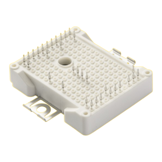
ST introduces the ACEPACK™ Power Module family, designed for easy mounting and reliable
performance in rugged applications. The available module form factors are ACEPACK™ 1 with 33.8 mm
x 48 mm and ACEPACK™ 2 with 56.7 mm x 48 mm body dimensions. Various die selections in silicon
and silicon carbide substrates can be housed in several configurations.
These modules feature a compact, fully isolated, low profile housing able to integrate very high power
density components in a low junction-to-case thermal resistance DBC. Power modules simplify the
design and increase reliability, while PCB size and system costs are optimized.
The following sections provide recommendations for the connection of these modules to a printed circuit
board (PCB) and mounting and dismounting methods to achieve adequate connections, reliability and
performance in typical applications.
Figure 1: ACEPACK™ 1 and ACEPACK™ 2
November 2017
DocID030935 Rev 1
1/16
www.st.com
Advertisement
Table of Contents

Related Manuals for ST ACEPACK 1


Summary of Contents for ST ACEPACK 1
- Page 1 Press-fit ACEPACK™ power modules mounting instructions Introduction ST introduces the ACEPACK™ Power Module family, designed for easy mounting and reliable performance in rugged applications. The available module form factors are ACEPACK™ 1 with 33.8 mm x 48 mm and ACEPACK™ 2 with 56.7 mm x 48 mm body dimensions. Various die selections in silicon and silicon carbide substrates can be housed in several configurations.
-
Page 2: Table Of Contents
Contents TN1250 Contents PCB requirements ................3 Module mounting process in a PCB ..........5 General press- in process ..............5 Multiple modules press-in process ............ 6 Fixing a PCB to the ACEPACK™ module ........8 Mounting the module to a heat sink ..........9 Requirements for a heat sink ............ -
Page 3: Pcb Requirements
TN1250 PCB requirements PCB requirements The press-fit used in the ACEPACK™ module has been qualified for standard FR4 printed circuit boards with tin (chemically) (IEC 60352-5 + IEC60747-15). If other handling technologies are used in the production of printed circuit boards, they would have to be tested, inspected and qualified. - Page 4 PCB requirements TN1250 Press-fit leads option Min. Typ. Max. Unit Metallization of circuit board Tin (chemically) / HAL Metallization of pin Tin (galvanic) Other tin finish technologies should be avoided before verification. The HAL plating method is not recommended because of uneven plating on the hole. The electrical and thermal contacts with the circuit board are implemented by means of cold welding when press-fit pins are used.
-
Page 5: Module Mounting Process In A Pcb
TN1250 Module mounting process in a PCB Module mounting process in a PCB General press- in process The press-fit process is a cost-effective way to assemble power modules without introducing additional thermal loads. The press-fit connection generates a strong mechanical and a good electrical connection between the module and the PCB. Figure 4: Types of equipment for press-in Generally, a module can be pressed in until the stand-offs on the four corners of the module touch the PCB. -
Page 6: Multiple Modules Press-In Process
Module mounting process in a PCB TN1250 Attention should also be paid to other components like resistors, diodes or capacitors that need to be assembled on the PCB area next to the ACEPACK™ module. PCB bending during press-in processes can cause mechanical stress to other PCB components. It is recommended to leave at least 4 mm between the edge of these components and the middle of the PTH. - Page 7 TN1250 Module mounting process in a PCB between the case and the PCB. The distance keepers and the other board components should be designed so that no contact among them can occur during the press-in process. The module and the PCB are first placed on the lower press-in tool and the module is then aligned to the PCB with the guide pins.
-
Page 8: Fixing A Pcb To The Acepack™ Module
Fixing a PCB to the ACEPACK™ module Figure 7: ACEPACK fixing PCB and cross-section Figure 8: Guide hole for the screws in ACEPACK 1 and ACEPACK 2 After the PCB mounting process, it is recommended to fix the PCB to the module with screws to ensure reliable contact. -
Page 9: Mounting The Module To A Heat Sink
TN1250 Mounting the module to a heat sink Mounting the module to a heat sink The heat produced by a module must be dissipated to avoid overheating and consequent damage. The thermal performance of a module in combination with a heat sink can be characterized by the sum of all thermal resistances along the thermal path: junction-to- case, case-to-heatsink,and heatsink-to-ambient, as shown in the figure below. - Page 10 Mounting the module to a heat sink TN1250 Figure 10: Screw clamping zone dimensions In the figure below shows one-step and three-step fastening methods. In the one-step method, the two screws are simultaneously fastened to avoid tilting on one side of module. It is recommended to synchronize the two electric screwdrivers with the same rpm and maximum torque.
- Page 11 TN1250 Mounting the module to a heat sink Figure 11: Module to heatsink fastening method Table 3: Technical data of the mounting screw Description Value Mounting screw 2.0 – 2.3 Nm Recommended mounting tourque DocID030935 Rev 1 11/16...
-
Page 12: Assembly Of The Pcb And Heat Sink
Assembly of the PCB and heat sink TN1250 Assembly of the PCB and heat sink After modules are assembled to the PCB and the heat sink, the overall structural integrity needs to be considered to avoid mechanical stress to any of the system components. If the PCB is large and heavy with other components assembled to it, there is some risk that the PCB can bend, creating mechanical stress on the module and the PCB. - Page 13 TN1250 Assembly of the PCB and heat sink Figure 13: Heat sink mounting DocID030935 Rev 1 13/16...
-
Page 14: Clearance And Creepage Distances
Clearance and creepage distances TN1250 Clearance and creepage distances When defining the layout of the PCB, application-specific standards, especially regarding clearance and creepage distances, must be considered. This is particularly important for the area of the screw clamp located under the printed circuit board. In order to meet the respective requirements regarding clearance and creepage distances, current carrying devices or through-holes in this area should be avoided, or additional isolation measures like lacquering must be taken. -
Page 15: Revision History
TN1250 Revision history Revision history Table 4: Document revision history Date Revision Changes 07-Nov-2017 Initial release. DocID030935 Rev 1 15/16... - Page 16 ST products and/or to this document at any time without notice. Purchasers should obtain the latest relevant information on ST products before placing orders. ST products are sold pursuant to ST’s terms and conditions of sale in place at the time of order acknowledgement.
Need help?
Do you have a question about the ACEPACK 1 and is the answer not in the manual?
Questions and answers