Table of Contents
Advertisement
Quick Links
AN4070
Application note
250 W grid connected microinverter
By Rosario Attanasio
Introduction
This application note describes the implementation of a 250 W grid connected DC-AC
system suitable for operation with standard photovoltaic (PV) modules. The design is
associated to the STEVAL-ISV003V1 demonstration board which demonstrates the
possibility of implementing a full microinverter solution (MIC) using STMicroelectronics
products.
In fact, both the components used to implement the power, control and communication
section belong to the product portfolio offered by STMicroelectronics.
The design is based on two power stages, namely, an interleaved isolated boost DC-DC
converter and a mixed frequency DC-AC converter. The control section is based on an
STM32F103xx microcontroller which ensures proper maximum power point tracking
(MPPT) on the input side of the system and decoupled control of the active and reactive
power on the output. The control algorithm has been developed to allow system operation
both with 230 V AC, 50 Hz grids and with 240 V AC, 60 Hz without any hardware
modifications. The connection to a 120 V AC, 50/60 Hz grid requires few hardware
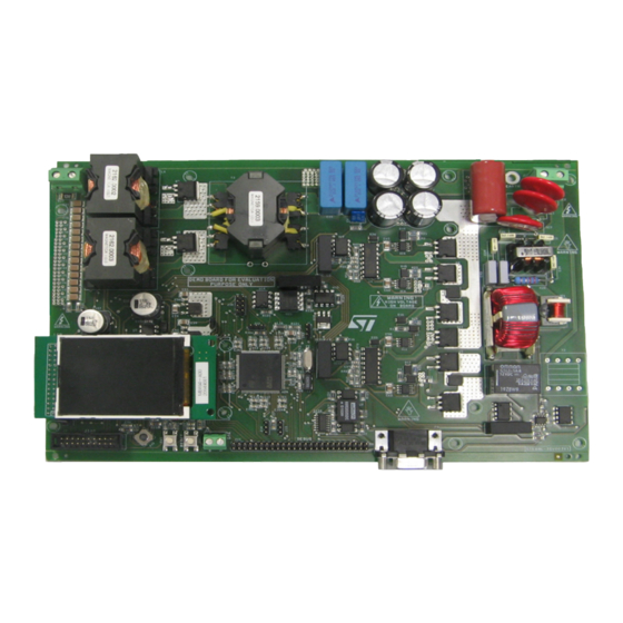
modifications to ensure the best system performance. An image of the STEVAL-ISV003V1
demonstration board is shown in
Figure
1.
Figure 1.
Image of the 250 W MIC
December 2012
Doc ID 022934 Rev 1
1/53
www.st.com
Advertisement
Table of Contents

Related Manuals for ST AN4070


Summary of Contents for ST AN4070
-
Page 1: Figure 1. Image Of The 250 W Mic
AN4070 Application note 250 W grid connected microinverter By Rosario Attanasio Introduction This application note describes the implementation of a 250 W grid connected DC-AC system suitable for operation with standard photovoltaic (PV) modules. The design is associated to the STEVAL-ISV003V1 demonstration board which demonstrates the possibility of implementing a full microinverter solution (MIC) using STMicroelectronics products. -
Page 2: Table Of Contents
Contents AN4070 Contents System description ......... . 5 DC-DC converter design . - Page 3 AN4070 List of tables List of tables Table 1. Summary of main electrical specifications ........6 Table 2.
- Page 4 List of figures AN4070 List of figures Figure 1. Image of the 250 W MIC ........... . 1 Figure 2.
-
Page 5: System Description
AN4070 System description System description The block diagram reported in Figure 2 shows the main concepts behind the proposed microinverter solution. Figure 2. Block scheme of the 250 W grid connected system AM12044v1 Although the characteristics of an MIC may change according to the modules’ electrical specifications, its structure can be composed by up to three stages to perform the MPPT function and deliver power to the grid. - Page 6 System description AN4070 The system is powered up by an auxiliary power supply which generates a +15 V and a +5 V bus from the input voltage using an L4951 integrated circuit and few external components. The startup voltage of the auxiliary power supply is 18 V while the maximum voltage is 55 V.
-
Page 7: Dc-Dc Converter Design
AN4070 DC-DC converter design DC-DC converter design The topology chosen for the DC-DC section of the MIC is an isolated, interleaved boost converter. The basic electrical scheme of such a converter is shown in Figure Figure 3. DC-DC converter topology... -
Page 8: Figure 4. Gate Driving Signals Of The Dc-Dc Converter
DC-DC converter design AN4070 Figure 4. Gate driving signals of the DC-DC converter Figure 5. Currents through the input inductors As the control strategy requires the two gate drive signals to be overlapped during part of the switching period, there is an operating interval during which both the MOSFET devices are ON and therefore both the input inductor chokes, L1 and L2, store energy. -
Page 9: Figure 6. Mosfet Mos1 And Mos2 Currents
AN4070 DC-DC converter design Figure 6. MOSFET MOS1 and MOS2 currents During the second switching interval MOS1 is still on while MOS2 is turned off. The energy, previously stored in L2 is now transferred to the secondary while inductor L1 is charged by the input voltage and its current continues to build up. -
Page 10: Figure 8. Hf Transformer Current
DC-DC converter design AN4070 Figure 8. HF transformer current The main specifications used for the design of the DC-DC stage are reported in Table Table 2. DC-DC converter main specifications Specification Value Nominal input voltage 35.8 V Maximum input voltage... - Page 11 AN4070 DC-DC converter design Calculation of the maximum duty cycle: In this topology the switch duty cycle is always >0.5. Let's call D the time beyond Ts/2 for which the MOSFET is still closed: Equation 2 − ⋅ ⋅ −...
- Page 12 DC-DC converter design AN4070 Calculation of input current ripple: Equation 9 Δ Δ Δ Δ ripple 10. Calculation of input inductors value: Equation 10 Δ Δ ⋅ ⋅ switch Δ ⋅ 11. Calculation of diodes RMS current: Equation 11 −...
-
Page 13: Table 3. Dc-Dc Converter Mosfet Main Characteristics
AN4070 DC-DC converter design 16. Calculation of diodes breakdown voltage: Equation 16 ⋅ ⋅ brdw diode 17. Calculation of input capacitor RMS current: Equation 17 Δ Δ ⋅ ⋅ 35000 35000 Δ Δ Ω Δ 18. MOSFET selection and losses calculations: Table 3. -
Page 14: Table 5. Hf Transformer Specifications
DC-DC converter design AN4070 HF transformer design The design is based on the specifications reported in Table 5 and has been used to provide the main parameters required by HF transformer manufacturers for the realization of the prototypes. Table 5. -
Page 15: Table 6. Rm14 Core With N87 Ferrite Main Characteristics
AN4070 DC-DC converter design Core selection: Based on the maximum power that the HF transformer has to manage, the RM14 core with N87 Ferrite from Epcos-TDK has been selected. The main characteristics of this core are reported in Table Table 6. - Page 16 DC-DC converter design AN4070 The maximum wire diameter to avoid skin effect is given by: Equation 25 δ Assuming a current density J of 5 A/mm^2: Equation 26 The primary and secondary wire selection can be done according to the following equation:...
-
Page 17: Figure 9. Basic Scheme Of The Dc-Ac Converter
AN4070 DC-DC converter design The second major contribution to transformer losses is given by core losses. The value of specific core loss, P , for an RM14 core operating at 35 kHz, 100 °C and with a maximum flux density of 200 mT, is equal to 141 kW/m^3. - Page 18 DC-DC converter design AN4070 The minimum value of capacitance required on the DC bus is calculated according to the following equation: Equation 34 − ⋅ ⋅ ⋅ ⋅ ⋅ where t is given by: Equation 35 ⋅ grid A total capacitance of about twice the calculated value, rated at 450 V and having an operating temperature of 105 °C, is selected for the inverter implementation.
-
Page 19: Table 7. Stb11N65M5 Mosfet Main Electrical Characteristics
AN4070 DC-DC converter design Choosing a filter capacitor value of 470 nF and a grid coupling inductor value equal to the filtering inductor value, the resulting filter resonant frequency is equal to 5.4 kHz which falls in the frequency range mentioned above. -
Page 20: Schematic Description
Schematic description AN4070 Schematic description This section of the application note is intended to provide information on the main circuits adopted in the MIC design. The two main power processing stages of the microinverter are shown in Figure 10. The input filter capacitance is realized with the parallel connection of fourteen, 100 V, 1 µF... - Page 21 AN4070 Schematic description connected between the gate and source of each inverter MOSFET. The supply voltage of the inverter gate drive circuit is provided by two isolated, integrated DC-DC converters whose input is the 5 V generated by the auxiliary power supply connected to the PV input.
-
Page 22: Figure 10. Schematic Of The Two Main Power Stages
Schematic description AN4070 Figure 10. Schematic of the two main power stages 22/53 Doc ID 022934 Rev 1... -
Page 23: Figure 11. Schematic Of The Filtering And Relay Circuit
AN4070 Schematic description Figure 11. Schematic of the filtering and relay circuit Doc ID 022934 Rev 1 23/53... -
Page 24: Figure 12. Dc-Dc Converter Driver
Schematic description AN4070 Figure 12. DC-DC converter driver 24/53 Doc ID 022934 Rev 1... -
Page 25: Figure 13. Dc-Ac Converter Driver
AN4070 Schematic description Figure 13. DC-AC converter driver Doc ID 022934 Rev 1 25/53... -
Page 26: Figure 14. Auxiliary Power Supply Of The Demonstration Board
Schematic description AN4070 Figure 14. Auxiliary power supply of the demonstration board Figure 15. AC line current sensing 26/53 Doc ID 022934 Rev 1... -
Page 27: Figure 16. Ac Line Voltage Sensing
AN4070 Schematic description Figure 16. AC line voltage sensing Doc ID 022934 Rev 1 27/53... -
Page 28: Figure 17. Pv Current Sensing
Schematic description AN4070 Figure 17. PV current sensing Figure 18. PV voltage sensing 28/53 Doc ID 022934 Rev 1... -
Page 29: Stm32F103Xx Based Current Control For Inverter Grid Connection
AN4070 STM32F103xx based current control for inverter grid connection STM32F103xx based current control for inverter grid connection The current control method is based on a d-q synchronous reference frame which provides both the advantage of zero steady-state error, thanks to the use of PI controllers, and simple implementation. -
Page 30: Figure 20. Implemented Pll Structure
STM32F103xx based current control for inverter grid connection AN4070 Equation 40 ⎡ ⎤ ⎡ ⎤ θ − θ ⎡ ⎤ β ⋅ ⎥ ⎢ ⎥ ⎢ ⎥ ⎢ θ θ ⎣ ⎦ ⎣ ⎦ ⎣ ⎦ α where: Equation 41 θ... - Page 31 AN4070 STM32F103xx based current control for inverter grid connection controlled transforming the current in the same reference frame and by acting on the amplitude of the I component. The I component must, also, be controlled in order to ensure zero reactive power injection. On the contrary, if the V...
-
Page 32: Figure 21. Block Diagram Of The Control Algorithm Implemented On The 250 W Mic Stm32F103Xx
STM32F103xx based current control for inverter grid connection AN4070 Figure 21. Block diagram of the control algorithm implemented on the 250 W MIC STM32F103xx Apart from gird connection and MPPT, some other functions are implemented for the correct operation of the conversion system. Here below a brief description of these functions: ●... - Page 33 AN4070 STM32F103xx based current control for inverter grid connection threshold of 440 V. In the case of bus DC under/overvoltage the system is disconnected from the grid according to the strategy already described. During normal operation the DC bus is regulated at 380 V.
- Page 34 STM32F103xx based current control for inverter grid connection AN4070 The tuning of the PI regulators can be performed using the specific function implemented in the control algorithm. Acting on the two current regulators is very effective in order to adjust the quality of the output current both in terms of total harmonic distortion.
-
Page 35: Experimental Test Results
AN4070 Experimental test results Experimental test results The typical voltage and current waveforms of both the DC-DC and DC-AC converter are shown in this section. In particular, Figure 22 shows the characteristic waveforms of the DC- DC converter MOSFETs, namely the drain to source MOSFET current (green track) and voltage (purple track). -
Page 36: Figure 23. Dc-Dc Converter Input Current Ripple Cancellation And Inductor Currents
Experimental test results AN4070 Figure 23. DC-DC converter input current ripple cancellation and inductor currents Figure 24. DC-DC converter HF transformer waveforms 36/53 Doc ID 022934 Rev 1... -
Page 37: Figure 25. Dc-Dc Converter Rectifier Diode Waveforms
AN4070 Experimental test results Figure 25. DC-DC converter rectifier diode waveforms Figure 26. Inverter modulating signals As already mentioned, the DC-AC converter has a hybrid modulation allowing one leg to switch at 17.4 kHz and one leg to switch at grid frequency. The image in... -
Page 38: Figure 27. Dc-Ac Converter Output Voltage And Current Waveforms
Experimental test results AN4070 and the DC-AC converter to be adjusted by acting on the duty cycle and modulating index respectively. The duty cycle has been adjusted to obtain a DC bus voltage of 390 V and the modulating index in order to get 230 V AC on the output for each test point. The efficiency... -
Page 39: Figure 28. Dc-Dc Converter Efficiency
AN4070 Experimental test results Figure 28. DC-DC converter efficiency Figure 29. Microinverter efficiency Doc ID 022934 Rev 1 39/53... -
Page 40: Figure 30. Mic Output Current And Voltage Waveforms During Grid Connection
Experimental test results AN4070 Figure 30. MIC output current and voltage waveforms during grid connection Figure 31. Output current THD% 40/53 Doc ID 022934 Rev 1... -
Page 41: Figure 32. Power Factor
AN4070 Experimental test results Figure 32. Power factor Doc ID 022934 Rev 1 41/53... -
Page 42: Appendix A Magnetic Components Datasheets
Magnetic components datasheets AN4070 Appendix A Magnetic components datasheets Figure 33. DC-DC boost converter inductors (part1) 06103 STP 04 Product Technical Specification Code : 2162.0003 Product: Inductor 600uH 4A Class Code: Customer: STMICROELECTRONICS Customer Code: Date Revision : 24.11.2010 Page 1 of 2... -
Page 43: Figure 34. Dc-Dc Boost Converter Inductors (Part2)
AN4070 Magnetic components datasheets Figure 34. DC-DC boost converter inductors (part2) 06103 STP 04 Product Technical Specification Code : 2162.0003 Product: Inductor 600uH 4A Class Code: Customer: STMICROELECTRONICS Customer Code: Date Revision Page 2 of 2 : 24.11.2010 DIMENSIONAL DRAWING... -
Page 44: Figure 35. Ac Voltage Tv
Magnetic components datasheets AN4070 Figure 35. AC voltage TV & & & AM12182v1 44/53 Doc ID 022934 Rev 1... -
Page 45: Figure 36. Dc-Dc Converter Hf Transformer (Part 1)
AN4070 Magnetic components datasheets Figure 36. DC-DC converter HF transformer (part 1) 06100 STP 22 Product Technical Specification Code: 2159.0003 Product: Switch Mode Transformer 250W 50kHz 1.9mH 200V Class Code: Customer: STMICROELECTRONICS Customer code: Date Revision Page 1 of 2... -
Page 46: Figure 37. Dc-Dc Converter Hf Transformer (Part 2)
Magnetic components datasheets AN4070 Figure 37. DC-DC converter HF transformer (part 2) 06100 STP 22 Product Technical Specification Code: 2159.0003 Product: Switch Mode Transformer 250W 50kHz 1.9mH 200V Class Code: Customer: STMICROELECTRONICS Customer code: Date Revision Page 2 of 2... -
Page 47: Figure 38. Inverter Filter Inductor (Part 1)
AN4070 Magnetic components datasheets Figure 38. Inverter filter inductor (part 1) 06272 STP 04 Product Technical Specification Code : 2196.0001 Product : Inductor 3.6mH Class Code: Date Revision Page 1 of 2 : 24.05.2011 TYPICAL APPLICATION T ECHNICAL DATA NDUCTOR FOR... -
Page 48: Figure 39. Inverter Filter Inductor (Part 2)
Magnetic components datasheets AN4070 Figure 39. Inverter filter inductor (part 2) 06272 STP 04 Product Technical Specification Code : 2196.0001 Product : Inductor 3.6mH Class Code: Date Revision Page 2 of 2 : 24.05.2011 DIMENSIONAL DRAWING -0.5 +0.1 26.5 0.71 ( 1.1 (... -
Page 49: Appendix B Alternative Dc-Dc Converter Magnetic Components With Low
AN4070 Alternative DC-DC converter magnetic components with low profile Appendix B Alternative DC-DC converter magnetic components with low profile Figure 40. DC/DC inductor for 250 W microinverter AM15526v1 Doc ID 022934 Rev 1 49/53... -
Page 50: Figure 41. Dc-Dc Transformer For 250 W Microinverter
Alternative DC-DC converter magnetic components with low profile AN4070 Figure 41. DC-DC transformer for 250 W microinverter " AM15527v1 50/53 Doc ID 022934 Rev 1... -
Page 51: Conclusions
AN4070 Conclusions Conclusions This application note describes the design and performance of a dual stage 250 W microinverter characterized by maximum power point tracking and active and reactive power control capability. This is the main reason why the power conversion is based on a dual stage topology rather than the more common single-stage one. -
Page 52: Revision History
Revision history AN4070 Revision history Table 8. Document revision history Date Revision Changes 12-Dec-2012 Initial release. 52/53 Doc ID 022934 Rev 1... - Page 53 No license, express or implied, by estoppel or otherwise, to any intellectual property rights is granted under this document. If any part of this document refers to any third party products or services it shall not be deemed a license grant by ST for the use of such third party products or services, or any intellectual property contained therein or considered as a warranty covering the use in any manner whatsoever of such third party products or services or any intellectual property contained therein.
Need help?
Do you have a question about the AN4070 and is the answer not in the manual?
Questions and answers