Table of Contents
Advertisement
Quick Links
Advertisement
Table of Contents

Related Manuals for Advantech SOM-2532 Series


Summary of Contents for Advantech SOM-2532 Series
- Page 1 User Manual SOM-2532...
- Page 2 No part of this manual may be reproduced, copied, translated, or transmitted in any form or by any means without the prior written permission of Advantech Co., Ltd. The information provided in this manual is intended to be accurate and reliable.
- Page 3 This product has passed the CE test for environmental specifications when shielded cables are used for external wiring. We recommend the use of shielded cables. This type of cable is available from Advantech. Please contact your local supplier for ordering information.
- Page 4 Document Feedback To assist us with improving this manual, we welcome all comments and constructive criticism. Please send all feedback in writing to support@advantech.com. Packing List Before system installation, check that the items listed below are included and in good condition.
- Page 5 In accordance with IEC 704-1:1982 specifications, the sound pressure level at the operator’s position does not exceed 70 dB (A). DISCLAIMER: These instructions are provided according to IEC 704-1 standards. Advantech disclaims all responsibility for the accuracy of any statements contained herein. SOM-2532 User Manual...
- Page 6 Safety Precaution - Static Electricity Follow these simple precautions to protect yourself from harm and the products from damage. To avoid electrical shock, always disconnect the power from the PC chassis before manual handling. Do not touch any components on the CPU card or other cards while the PC is powered on.
-
Page 7: Table Of Contents
1.3.10 Power Management..............8 1.3.11 Environment.................. 8 1.3.12 MTBF .................... 9 1.3.13 OS Support (duplicate with SW chapter) ........9 1.3.14 Advantech iManager ..............9 1.3.15 Power Consumption..............9 1.3.16 Performance ................. 9 1.3.17 Selection Guide w/ P/N ............... 10 1.3.18 Packing list.................. - Page 8 3.2.1 Main Setup.................. 21 Figure 3.2 Main Setup Screen........... 21 3.2.2 Advanced BIOS Features Setup..........22 Figure 3.3 Advanced BIOS Features Setup Screen....22 Figure 3.4 CPU Configuration ........... 23 Figure 3.5 PCH-FW Configuration..........24 Figure 3.6 Firmware Update Configuration ....... 25 Figure 3.7 Intel®Time coordinated computing......
- Page 9 Driver Installation ..................74 4.2.1 Windows Driver Setup (TBD)............74 4.2.2 Other OS..................74 Advantech iManager (SUSI 4.0) ............. 75 Appendix A Pin Assignment .........77 SOM-2532 Pin Assignment..............78 Appendix B Watchdog Timer ........87 Programming the Watchdog Timer ............88...
- Page 10 SOM-2532 User Manual...
-
Page 11: Chapter 1 General Information
Chapter General Information This chapter details background information on the SOM-2532 CPU Computer on Module. Sections include: Introduction Functional Block Diagram Product Specification... -
Page 12: Introduction
Introduction Advantech’s SOM-2532 series features SMARC 2.1.1 specifications and is equipped with the newest generation of Intel® processors — including the Pentium®, Cele- ron®, and Atom® platforms. SOM-2532 is designed with up to 4 cores and yields 40% better CPU performance and improved graphics processing when compared with previous models. -
Page 13: Functional Block Diagram
Inter Integrated Circuit – 2 wire (clock and data) signaling scheme allowing communication between integrated circuit, primarily used to read and load reg- ister values. Management Engine “Personal Computer – Advanced Technology” – an IBM trademark term used to PC-AT refer to Intel based personal computer in 1990s. -
Page 14: Product Specifications
Product Specifications 1.3.1 Compliance SMARC (Smart Mobility Architecture) 2.1 Basic Size – 82 x 50 mm (3.22 x 1.96 in) 1.3.2 Feature List Feature Min/Max in SMARC2.1 SOM-2532 Memory LPDDR4 eMMC (on module) 0/(N/A) LVDS LCD/eDP/MIPI-DSI 1/1/1 1/1/1 HDMI/DP++ DP++ MIPI-CSI... -
Page 15: Processor System
1.3.3 Processor System Std. Freq. Max. Turbo Freq. Core Cache (MB) TDP(W) Pentium®N6415 1.2 GHz 3.0 GHz Atom®x6211E 1.3 GHz 3.0 GHz Atom®x6413E 1.5 GHz 3.0 GHz Atom®x6425E 2.0GHz 3.0 GHz Atom®x6425RE 1.9GHz 1.3.4 Memory Dual channels onboard LPDDR4 3200MT/s up to 16GB, up to 4267MT/s by specific SPU SKUs (non-ECC) 1.3.5 Graphics/Audio... - Page 16 1.3.9.2 SATA Support 1 x ports SATA3.0 (6.0 Gb/s). 1.3.9.3 USB 3.2 /USB 2.0 2 x ports USB 3.2(10.0 Gaps) and 6 x ports USB 2.0 (480Mbps, include 1 client port) which are backward compatible to USB 1. 1.3.9.4 USB 3.2 SMARC SMARC USB_0_1_OC...
- Page 17 1.3.9.15 Supports TPM 2.0 module by default 1.3.9.16 Watchdog Support multi-level watchdog time-out output. Provides 1-65535 level, from 100ms to 109.22 minutes interval. 1.3.9.17 Serial port 2 x ports 4-wire and 2 x ports 2-wire HSUART signal interface using RTS/CTS control only Programmable FIFO enable/disable ...
-
Page 18: Power Management
1.3.10.5 Advantech S5 ECO Mode (Deep Sleep Mode) Advantech iManager provides additional features that allow the system to enter a very low suspend power mode – S5 ECO mode. In this mode, the module will cut all power, including suspend and active power, into the chipset and keep an on-module controller active. -
Page 19: Mtbf
1.3.12 MTBF Please refer Advantech SOM-2532 Series Reliability Prediction Report No: TBD. (Estimated date: 2021 Q4). 1.3.13 OS Support (duplicate with SW chapter) To install the drivers, please connect to the Internet and go to the following website: http://support.advantech.com.tw to download the setup file. -
Page 20: Selection Guide W/ P/N
The layout checklist will specify the layout constraints and recommendations for trace length, impedance, and other necessary information during design. Please contact the nearest Advantech branch office to acquire the design documents and/or advanced support. ... -
Page 21: Chapter 2 Mechanical Information
Chapter Mechanical Information This chapter details mechanical information on the SOM-2532 CPU Computer on Module. Sections include: Board Information Mechanical Drawing Assembly Drawing... -
Page 22: Board Information
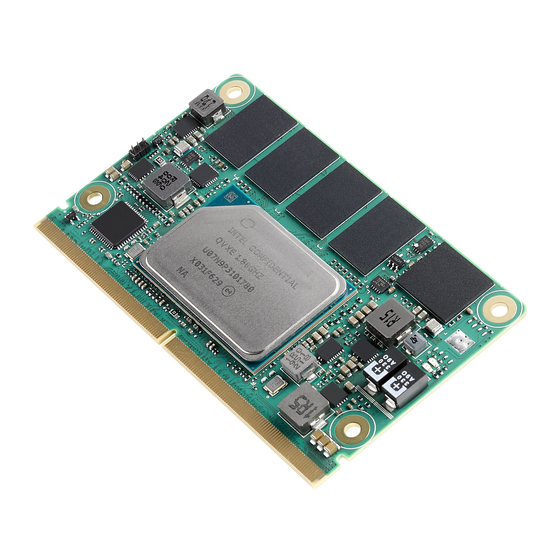
Board Information The figures below indicate the main chips on SOM-2532 Computer-on-Module. Please be aware on these positions while designing carrier boards to avoid mechani- cal issues and to choose thermal solutions that provide the best thermal dissipation performance. Figure 2.1 Atom®_QVXE Board Chip - Front Figure 2.2 Atom®_QVXE Board Chip - Rear SOM-2532 User Manual... -
Page 23: Mechanical Drawing
Mechanical Drawing For more details on 2D/3D models, please look on Advantech’s COM support service website http://com.advantech.com. Figure 2.3 Atom Series Board Mechanical Diagram - Front Figure 2.4 Atom Series Board Mechanical Diagram - Rear Figure 2.5 Atom Series Board Mechanical Diagram -Side... - Page 24 Figure 2.6 Celeron_Pentium_J_N Series Board Mechanical Diagram - Front Figure 2.7 Celeron_Pentium_J_N Series Board Mechanical Diagram – Rear Figure 2.8 Celeron_Pentium_J_N Series Board Mechanical Diagram – Side SOM-2532 User Manual...
-
Page 25: Assembly Drawing
Assembly Drawing These figures demonstrate the assembly order of the thermal module — in particular the COM module to carrier board. Figure 2.9 Atom Series Assembly Diagram SOM-2532 User Manual... - Page 26 Figure 2.10 Celeron_Pentium_J_N Series Board Assembly Diagram There are 4 x reserved screw holes for SOM-2532. These are used to attach the heat spreader. SOM-2532 User Manual...
- Page 27 Please consider the CPU and chip height tolerance when designing your thermal solution. Intel Atom® Processor Series Figure 2.11 Main Chip Height and Tolerance Intel® Pentium and Celeron N and J Series Processors Figure 2.12 Main Chip Height and Tolerance SOM-2532 User Manual...
- Page 28 SOM-2532 User Manual...
-
Page 29: Chapter 3 Ami Bios
Chapter AMI BIOS This chapter details BIOS setup information for the SOM-2532 CPU computer-on module. Sections include: Introduction Entering Setup Hot/Operation Key Exit BIOS Setup Utility... -
Page 30: Introduction
Introduction AMI BIOS has been integrated into many motherboards for over a decade. With the AMI BIOS Setup Utility, users can modify BIOS settings and control various system features. This chapter describes the basic navigation of the BIOS Setup Utility. Figure 3.1 Setup Program Initial Screen AMI's BIOS ROM has a built-in Setup program that allows users to modify the basic system configuration. - Page 31 3.2.1 Main Setup When users first enter the BIOS Setup Utility, users will enter the Main setup screen. Users can always return to the Main setup screen by selecting the Main tab. There are two Main Setup options. They are described in this section. The Main BIOS Setup screen is shown below.
- Page 32 3.2.2 Advanced BIOS Features Setup Select the Advanced tab from the SOM-2532 setup screen to enter the Advanced BIOS Setup screen. Users can select any item in the left frame of the screen, such as CPU Configuration, to go to the sub menu for that item. Users can display an Advanced BIOS Setup option by highlighting it using the <Arrow>...
- Page 33 3.2.2.1 CPU Configuration Figure 3.4 CPU Configuration Speed Displays the Processor Speed Intel (VMX) Virtualization Technology When enabled, a VMM can utilize the additional hardware capabilities provided by Vanderpool Technology Active Processor Cores Number of cores to enable in each processor package ...
- Page 34 3.2.2.2 PCH-FW Configuration Figure 3.5 PCH-FW Configuration ME State When Disabled ME will be put into ME Temporarily Disabled Mode ME Unconfig on RTC Clear When Disabled ME will nor unconfigured on RTC clear Firmware Update Configuration Configure Management Engine Technology Parameters OEM Key Revocation Configuration ...
- Page 35 3.2.2.3 Firmware Update Configuration Figure 3.6 Firmware Update Configuration ME FW Image Re-Flash Enable/Disable Me FW Image Re-Flash function. FW Update Enable/Disable Me FW Update function. SOM-2532 User Manual...
- Page 36 3.2.2.4 Intel®Time coordinated computing Figure 3.7 Intel®Time coordinated computing IO Fabric Low Latency Enable or Disable IO Farbic Low Latency. This will turn off some power manage- ment in the PCH IO fabrics. This option provides the most aggressive IO Fabric performance setting.
- Page 37 RAPL PL1 enable Enable=enable, Disable(Disable=Def) RAPL PL2 enable Enable=enable, Disable(Disable=Def) Power down mode CKE Power down Mode Control RC6(Render standby) Check to enable render standby support Legacy IO low latency Set to enable low latency of legacy Io. Some systems require lower IO latency irrespective of power.
- Page 38 Enable/Disable Precision Time Measurement Multi-VC Enable/Disalbe Multi Virtual Channel. 3.2.2.5 Trusted Computing Figure 3.9 Trusted Computing Security Device Support Enables or Disables BIOS support for security device. The OS will not show Security Device. TCG EFI protocol and INT1A interface will not be available SHA-1 PCR Bank ...
- Page 39 Select to Tell O.S. to support PPI Spec Version 1.2 or 1.3. Note some HCK tests might not support 1.3. TPM2.0 Interface Type Select the communication interface to TPM2.0 device Device select TPM1.2 will restrict support to TPM1.2 devices, TPM2.0 will restrict support to TPM2.0 devices, Auto will support both with the default set to TPM2.0 devices if not found, TPM1.2 devices will enumerated 3.2.2.6...
- Page 40 3.2.2.7 Embedded Controller Figure 3.11 Embedded Controller CPU Shutdown Temperature CPU Shutdown Temperature Smart Fan – Carrier Board Control Carrier Board Smart FAN function. Get value from EC and only set value when Save Changes. Backlight Enable Polarity ...
- Page 41 3.2.2.8 Serial Port 1 Configuration Figure 3.12 Serial Port 1 Configuration Serial Port Enable or Disable Serial Port (COM) Device Settings Set Parameters of Serial Port 1 (COMA) Change Settings Select an optimal settings for Super IO Device Device Mode ...
- Page 42 3.2.2.9 Serial Port 2 Configuration Figure 3.13 Serial Port 2 Configuration Serial Port Enable or Disable Serial Port (COM) Device Settings Set Parameters of Serial Port 2 (COMB) Change Settings Select an optimal settings for Super IO Device Device Mode ...
- Page 43 3.2.2.10 Hardware Monitor Figure 3.14 Hardware Monitor 3.2.2.11 Serial Port Console Redirection Figure 3.15 Serial Port Console Redirection SOM-2532 User Manual...
- Page 44 COM0 Console Redirection Console Redirection Enable or Disable. Console Redirection Settings The settings specify how the host computer and the remote computer (which the user is using) will exchange data. Both computers should have the same or compatible settings. COM1 Console Redirection ...
- Page 45 3.2.2.12 USB Configuration Figure 3.16 USB Configuration Legacy USB support Enables Legacy USB support. AUTO option disables legacy support if no USB devices are connected. DISABLE option will keep USB devices available only for EFI applications. XHCI hand-off This is a workaround for OS without XHCI hand-off support.
- Page 46 3.2.2.13 Network Stack Configuration Figure 3.17 Network Stack Configuration Network Stack Enable/Disable UEFI Network Stack IPv4 PXE support Enable/Disable IPv4 PXE boot support. If disabled, IPv4 PXE boot support will not be available IPv4 HTTP Support Enable/Disable IPv4 HTTP boot support. If disabled, IPv4 HTTP boot support will not be available IPv6 PXE Support ...
- Page 47 3.2.2.14 SDIO Configuration Figure 3.18 SDIO Configuration SDIO Access Mode Auto Option: Access SD device in DMA mode if the controller supports it, other- wise in PIO mode.DMA Option: Access SD device in DMA mode.PIO Option: Access SD device in PIO mode. eMMC S0J57X SOM-2532 User Manual...
- Page 48 3.2.2.15 SMARC GPIO Configuration Figure 3.19 Network Stack Configuration GPIO0 SMARC GPIO0 GPIO1 SMARC GPIO1 GPIO2 SMARC GPIO2 GPIO3 SMARC GPIO3 GPIO4 SMARC GPIO4 GPIO5 SMARC GPIO5 GPIO6 SMARC GPIO6 SOM-2532 User Manual...
- Page 49 3.2.3 Chipset Setup Select the chipset tab from the SOM-2532 setup screen to enter the chipset BIOS Setup screen. You can display a chipset BIOS setup option by highlighting it using the <Arrow> keys. All Plug and Play BIOS setup options are described in this section. The Plug and Play BIOS Setup screen is shown below.
- Page 50 3.2.3.1 System Agent (SA) Configuration Figure 3.21 System Agent (SA) Configuration Memory Configuration Memory Configuration Parameters VT-d VT-d capability Above 4GB MMIO BIOS assignment Enable/Disable above 4GB memory mapped IO BIOS assignment. This is enabled automatically when aperture size is set to 2048MB. SOM-2532 User Manual...
- Page 51 Memory Configuration Figure 3.22 Memory Configuration – Max TOLUD Maximum value of TOLUD. Dynamic assignment would adjust TOLUD auto- matically based on the largest MMIO length of installed graphic controller Graphics Configuration Figure 3.23 Graphics Configuration SOM-2532 User Manual...
- Page 52 – Internal Graphics Keep IGFX enabled base on the setup options – GTT Size Select the GTT size – Aperture Size Select the aperture size. Note: Above 4GB MMIO BIOS assignment is atomi- cally enabled when selecting 2048MB aperture. To use this feature, please disable CSM support.
- Page 53 – LVDS swing level LVDS swing level – Primary IGFX Boot Display Select the video device which will be activated during POST. This has no effect if external graphics present. Secondary boot display selection will appear based on your selection. VGA modes will be supported only on pri- mary display –...
- Page 54 PSE Configuration Programmable service engine configuration TSN GBE Configuration Time sensitive network GBE configuration PCI Express Configuration Figure 3.26 PCI Express Configuration – DMI Link ASPM Control The control of Active State Power Management of theDMI Link –...
- Page 55 – PCI Express Root Port 1 Figure 3.27 PCI Express Root Port 1 – PCI Express Root Port 1 Control the PCI Express Root Port. AUTO: To disable unused root port auto- matically for the most optimum power savings. Enable: Enable PCIe root port Disable: Disable PCIe root port –...
- Page 56 – PCI Express Root Port 2 Figure 3.28 PCI Express Root Port 2 – PCI Express Root Port 2 Control the PCI Express Root Port. AUTO: To disable unused root port auto- matically for the most optimum power savings. Enable: Enable PCIe root port Disable: Disable PCIe root port –...
- Page 57 – PCI Express Root Port 3 Figure 3.29 PCI Express Root Port 3 – PCI Express Root Port 3 Control the PCI Express Root Port. AUTO: To disable unused root port auto- matically for the most optimum power savings. Enable: Enable PCIe root port Disable: Disable PCIe root port –...
- Page 58 – PCI Express Root Port 4 Figure 3.30 PCI Express Root Port 4 – PCI Express Root Port 4 Control the PCI Express Root Port. AUTO: To disable unused root port auto- matically for the most optimum power savings. Enable: Enable PCIe root port Disable: Disable PCIe root port –...
- Page 59 SATA Configuration Figure 3.31 SATA Configuration SATA Controller(s) Enable/Disable SATA Device. SATA Controller Speed Indicates the maximum speed the SATA controller can support. SATA Port 1 Port 1 Enable or Disable SATA Port Hot plug ...
- Page 60 USB Configuration Figure 3.32 USB Configuration – XHCI Disable Compliance Mode Options to disable Compliance Mode. Default is False which does not disable Compliance Mode. Set to TRUE to disable Compliance Mode. – XDCI Support Enable/Disable XDCI SOM-2532 User Manual...
- Page 61 Security Configuration Figure 3.33 Security Configuration – RTC Memory Lock Enable will lock bytes 38h-3Fh in the lower/upper 126 –byte bank of RTC – BIOS Lock Enable/Disable the PCH BIOS lock enable feature. Required to be enabled to ensure SMM protection of flash SOM-2532 User Manual...
- Page 62 HD Audio Subsystem Configuration Settings Figure 3.34 HD Audio Subsystem Configuration Settings – HD Audio Control Detection of the HD-Audio device. Disabled=HDA will be uncondi- tionally disabled. Enabled=HAD will be unconditionally enabled. – Audio DSP Enable/Disable Audio DSP SOM-2532 User Manual...
- Page 63 SerialIO Configuration Figure 3.35 SerialIO Configuration – I2C0 controller Enables/Disables serialio controller. If given devices is function0 PSF dis- abling is skipped. PSF default will remain and device PCI CFG space will still be visible. This is needed to allow PCI enumerator access functions above 0 in a multifunction device –...
- Page 64 be visible. This is needed to allow PCI enumerator access functions above 0 in a multifunction device – Serial IO I2C0 Settings Figure 3.36 Serial IO I2C0 Settings – Set Serial IO I2C #0 Speed Select serial IO I2C#0 speed SOM-2532 User Manual...
- Page 65 – Serial IO I2C2 Settings Figure 3.37 Serial IO I2C2 Settings – Set Serial IO I2C #2 Speed Select serial IO I2C#2 speed – Serial IO I2C3 Settings Figure 3.38 Serial IO I2C3 Settings SOM-2532 User Manual...
- Page 66 – Set Serial IO I2C #3 Speed Select serial IO I2C#3 speed – Serial IO I2C4 Settings Figure 3.39 Serial IO I2C4 Settings – Set Serial IO I2C #4 Speed Select serial IO I2C#4 speed SOM-2532 User Manual...
- Page 67 – Serial IO SPI1 Settings Figure 3.40 Serial IO SPI1 Settings – Chipselect 0 polarity Sets initial polarity for chipselect signal – Chipselect 1 polarity Sets initial polarity for chipselect signal – Delayed Rx Clock Configure the SPI delayed Rx clock option: As is –Default internal-Internally delayed Tx Clock-Negative edge of Tx clock Rx Clock-Negative edge of delayed Ex clock –...
- Page 68 – SCS Configuration – eMMC 5.1 Controller Enable or Disable SCS eMMC 5.1 Controller – eMMC 5.1 HS400 Mode Enable or Disable SCS eMMC 5.1 HS400 Mode – Enable HS400 software tuning Software tuning should improve eMMC HS400 stability at the expense of boot time –...
- Page 69 – Serial IO UART0 Settings Figure 3.41 Serial IO UART0 Settings – Hardware flow control When enabled configures additional 2 GPIO pads for use as RTS/CTS sig- nals for UART – DMA enable Enabled: UART OS driver will use DMA when possible. Disable: OS driver will enforce PIO mode SOM-2532 User Manual...
- Page 70 Serial IO UART2 Settings Figure 3.42 Serial IO UART2 Settings – Hardware flow control When enabled configures additional 2 GPIO pads for use as RTS/CTS sig- nals for UART – DMA enable Enabled: UART OS driver will use DMA when possible. Disable: OS driver will enforce PIO mode SOM-2532 User Manual...
- Page 71 PSE Controller Figure 3.43 PSE Controller – PSE controller Enables /Disables programmable service engine device – Shell Enable/Disable shell – Eclite Enable/Disable PSE Eclite service – Enable/Disable OOB service – Enable/Disable PSE GBE WoL – PSE Debug(JTAG/SWD)Enable PSE JTAG/SWD Debug enable –...
- Page 72 grayed out, check the above options. The same pin cannot be assigned to multiple IP. I2S1 does not have conflict – UART0 If UART0 is disabled, UART1-5 will be disabled too due to sharing same function – HSUART0/RS485 Select this to enable UART to support HSUART/RS485. Each HSUART pin conflict dependency is similar to UART –...
- Page 73 HSUART3/RS485 Select this to enable UART to support HSUART/RS485. Each HSUART pin con- flict dependency is similar to UART UART4 To assign this device to host owned, you must enable PSE UART0 to host owned because UART0 is the function0 of this device. UART0 has no pin con- flict.
- Page 74 I2C5 To assign this device to host owned, you must enable PSE I2C0 to host owned because I2C0 is the function 0 of this device. I2C1 has pin conflict with TGPIO8- 9, I2C2 has no pin conflict. I2C3 has pin conflict with TGPIO18-19.I2C4 has no pin conflict.
- Page 75 SPI2 SPI2 has pin conflict with WWAN WAKE GPIO. If it is grayed out, check the WWAN Wake GPIO configuration or serial IO SPI0. The same pin cannot be assigned to multiple IP. SPI3 To assign this device to host owned, you must enable PSE SPI0 to host owned because SPI0 is the function 0 of this device.
- Page 76 Figure 3.46 PSE Controller GPIO/TGPIO1 Owner of GPIO/TGPIO 1 controller(PSE or HOST owned) GPIO/TGPIO 1 Mux selection Choose Top, Mid, Lower of all mux for GPIO/TGPIO 1 controller instance. Lower: TGPIO(30-49) GPIO(50-59) Mid: TGPIO(30-39, 50-59)GPIO(40-49) Top: TGPIO(40-59) GPIO(30-39) All:GPIO(30-59) GPIO/TGPIO 1 Pin selection Enable individual GPIO/TGPIO pin PSE Interrupt assignment configuration Checked=Interrupt set to SB mode.
- Page 77 Checked=Interrupt set to SB mode. Default unchecked is MSI mode UART5 Checked=Interrupt set to SB mode. Default unchecked is MSI mode HSUART0 Checked=Interrupt set to SB mode. Default unchecked is MSI mode HSUART1 Checked=Interrupt set to SB mode. Default unchecked is MSI mode HSUART2 Checked=Interrupt set to SB mode.
- Page 78 QEP3 Checked=Interrupt set to SB mode. Default unchecked is MSI mode I2C0 Checked=Interrupt set to SB mode. Default unchecked is MSI mode I2C1 Checked=Interrupt set to SB mode. Default unchecked is MSI mode I2C2 Checked=Interrupt set to SB mode. Default unchecked is MSI mode I2C3 Checked=Interrupt set to SB mode.
- Page 79 TSN GBE configuration Figure 3.48 TSN GBE configuration – PCH TSN LAN Controller Enable/Disable TSN LAN – PCH TSN GBE Multi-Vc Enable/Disable TSN Multi Virtual Channels – PCH TSN GBE SGMII Support Enable/Disable SGMII mode for PCH TSN GBE. Ports in SGMII mode with the same PLL common lane must use the same link speed.
- Page 80 Speed. SATA or UFS may need to be disabled if TSN port is using the same PLL common lane. Please make sure IFWI has proper straps set for SGMII. Make sure Flex IO Lane Assignment is not NONE. – PSE TSN GBE 1 Link Speed PSE TSN GBE 1 Link Speed configuration.
- Page 81 Boot Setup Figure 3.50 Boot Setup Boot Configuration – Setup Prompt Timeout Number of seconds to wait for setup activation key. 65535(0xFFFF) means indefinite waiting. – Bootup NumLock State Select the keyboard NumLock state – Quiet Boot Enables or disables Quiet Boot option –...
- Page 82 3.2.5 Save & Exit Figure 3.51 Save & Exit Save Options Save Changes and Exit3.4.1 Exit system setup after saving the changes. Discard Changes and Exit Exit system setup without saving any changes. Save Changes and Reset ...
- Page 83 Chapter S/W Introduction and Installation S/W Introduction Driver Installation Advantech iManager (SUSI 4)
-
Page 84: Driver Installation
S/W Introduction The mission of Advantech Embedded Software Services is to "Enhance quality of life with Advantech platforms and Microsoft Windows embedded technology" We enable Windows Embedded software products on Advantech platforms to more effectively support the embedded computing community. Customers are freed from the hassle of dealing with multiple vendors (Hardware suppliers, System integrators, Embedded OS distributor) for projects. -
Page 85: Advantech Imanager (Susi 4.0)
It makes these embedded features easier to integrate, speed up develop- ing schedule, and provide the customer’s software continuity while upgrade hard- ware. More details of how to use the APIs and utilities, please refer to Advantech iManager 2.0 Software API User Manual. - Page 86 SOM-2532 User Manual...
-
Page 87: Appendix A Pin Assignment
Appendix Pin Assignment This appendix gives you the infor- mation about the hardware pin assignment of the SOM-2532 CPU System on Module. Sections include: SOM-2532 Pin Assignment... -
Page 88: Som-2532 Pin Assignment
SOM-2532 Pin Assignment This section gives SOM-2532 pin assignment on SMARC connector which compliant with SMARC 2.0 definitions. Please contact Advantech for a design guide, checklist, reference schematic, hardware/software, and/or detailed information. SMARC Function Pin Name SOM-2532 S125 LVDS0_0+ / eDP0_TX0+ /DSI0_D0+... - Page 89 DP1_LANE0+ / HDMI_D2+ DP1_LANE0- / HDMI_D2- DP1_LANE1+ / HDMI_D1+ DP1_LANE1- / HDMI_D1- DP1_LANE2+ / HDMI_D0+ DP1_LANE2- / HDMI_D0- DP++ over HDMI P101 DP1_LANE3+ / HDMI_CK+ P102 DP1_LANE3- / HDMI_CK- P104 DP1_HPD / HDMI_HPD P105 DP1_AUX- / HDMI_CTRL_DAT P106 DP1_AUX+ / HDMI_CTRL_CK P107 DP1_AUX_SEL S102...
- Page 90 P108 GPIO0 / CAM0_PWR# P109 GPIO1 / CAM1_PWR# P110 GPIO2 / CAM0_RST# P111 GPIO3 / CAM1_RST# I2C_CAM0_DAT I2C_CAM0_CK I2C_CAM1_DAT I2C_CAM1_CK CSI0_RX0+ CSI0_RX0- CSI0_RX1+ CSI0_RX1- CSI1_RX0+ CSI1_RX0- CSI1_RX1+ CSI1_RX1- CSI1_RX2+ CSI1_RX2- CSI1_RX3+ CSI1_RX3- CSI0_CK+ CSI0_CK- CSI1_CK+ CSI1_CK- CAM_MCK SDIO_D0 SDIO_D1 SDIO_D2 SDIO_D3 SDIO Card SDIO_CMD...
- Page 91 ESPI_CK / SPI1_ CK / QSPI_CK v / -/- ESPI_CS0# / SPI1_CS0# / QSPI_CS0# v / -/- ESPI_CS1# / SPI1_CS1# / QSPI_CS1# v / -/- ESPI_IO_1 / SPI1_DIN / QSPI_IO_1 v / -/- ESPI_IO_0 / SPI1_DO /QSPI_IO_0 v / -/- eSPI/SPI1 ESPI_IO_2 / QSPI_IO_2 v / -...
- Page 92 USB0+ USB0- USB1+ USB1- USB2+ USB2- USB3+ USB3- USB4+ USB4- USB5+ USB5- USB0_EN_OC# USB1_EN_OC# USB2_EN_OC# USB3_EN_OC# USB4_EN_OC# USB5_EN_OC# USB0_VBUS_DET USB3_VBUS_DET USB0_OTG_ID S104 USB3_OTG_ID USB2SSRX- USB2SSRX+ USB3SSRX- USB3SSRX+ USB2SSTX- USB2SSTX+ USB3SSTX- USB3SSTX+ SOM-2532 User Manual...
- Page 93 PCIE_A_TX+ PCIE_A_TX- PCIE_B_TX+ PCIE_B_TX- PCIE_C_TX+ / SERDES_1_TX+ v / v PCIE_C_TX- / SERDES_1_TX- v / v PCIE_D_TX+ / SERDES_0_TX+ v / v PCIE_D_TX- / SERDES_0_TX- v / v PCIE_A_RX+ PCIE_A_RX- PCIE_B_RX+ PCIE_B_RX- PCIE_C_RX+ / SERDES_1_RX+ v / v PCIe PCIE_C_RX- / SERDES_1_RX v / v PCIE_D_RX+ / SERDES_0_RX+ v / v...
- Page 94 GBE0_MDI0+ GBE0_MDI0- GBE0_MDI1+ GBE0_MDI1- GBE0_MDI2+ GBE0_MDI2- GBE0_MDI3+ GBE0_MDI3- GBE1_MDI0+ GBE1_MDI0- GBE1_MDI1+ GBE1_MDI1- GBE1_MDI2+ Ethernet GBE1_MDI2- GBE1_MDI3+ GBE1_MDI3- GBE0_LINK100# GBE0_LINK100# GBE0_LINK1000# GBE1_LINK1000# GBE0_LINK_ACT# GBE1_LINK_ACT# GBE0_CTREF GBE1_CTREF GBE0_SDP GBE1_SDP Watchdog S145 WDT_TIME_OUT# P108 GPIO0 / CAM0_PWR# v / - P109 GPIO1 / CAM1_PWR# v / - P110 GPIO2 / CAM0_RST#...
- Page 95 S150 VIN_PWR_BAD# S154 CARRIER_PWR_ON S153 CARRIER_STBY# P126 RESET_OUT# P127 RESET_IN# P128 POWER_BTN# S149 SLEEP# Management Pins S148 LID# S156 BATLOW# P122 I2C_PM_DAT P121 I2C_PM_CK S151 CHARGING# S152 CHARGER_PRSNT# S157 TEST# SMB_ALERT P123 BOOT_SEL0# P124 BOOT_SEL0# Boot Select P125 BOOT_SEL2# S155 FORCE_RECOV# S147 VDD_RTC...
- Page 96 P100 P103 P120 P133 P142 Power / GND /RSVD S101 S110 S119 S124 S130 S136 S143 RSVD RSVD RSVD RSVD RSVD RSVD RSVD S123 RSVD S142 RSVD S158 RSVD VDD_JTAG_IO JTAG_TRST# JTAG_TMS JTAG JTAG_TDO JTAG_TDI JTAG_TCK SOM-2532 User Manual...
-
Page 97: Appendix B Watchdog Timer
Appendix Watchdog Timer This appendix details information about the watchdog timer pro- gramming on the SOM-2532 CPU System on Module. Sections include: Watchdog Timer Programming... -
Page 98: Programming The Watchdog Timer
Programming the Watchdog Timer Trigger Event Note (BIOS setting default disable)** Power button event Power Off Support H/W Restart Support WDT Pin Activate Support ** WDT new driver support automatically select available IRQ number from BIOS, and then set to EC. Only Win10 support it. In other OS, it will still use IRQ number from BIOS setting as usual. -
Page 99: Appendix C System Assignments
Appendix System Assignments This appendix details information on the system resource alloca- tion on the SOM-2532 CPU Sys- tem on Module. Sections include: System I/O ports DMA Channel Assignments Interrupt Assignments 1st MB Memory Map... -
Page 100: System I/O Ports
System I/O Ports Table C.1: System I/O Ports Resource Device 0x00000000-0x00000CF7 PCI Express Root Complex 0x00000020-0x00000021 Programmable interrupt controller 0x00000024-0x00000025 Programmable interrupt controller 0x00000028-0x00000029 Programmable interrupt controller 0x0000002C-0x0000002D Programmable interrupt controller 0x0000002E-0x0000002F Motherboard resources 0x00000030-0x00000031 Programmable interrupt controller 0x00000034-0x00000035 Programmable interrupt controller 0x00000038-0x00000039 Programmable interrupt controller 0x0000003C-0x0000003D... -
Page 101: Interrupt Assignments
Table C.1: System I/O Ports 0x00003080-0x00003083 Standard SATA AHCI Controller 0x00003090-0x00003097 Standard SATA AHCI Controller 0x0000EFA0-0x0000EFBF Intel® SMBus Controller - 4B23 Interrupt Assignments Table C.2: Interrupt Assignments Resource Device IRQ 0 System timer IRQ 3 Communications Port (COM2) IRQ 7 Communications Port (COM1) IRQ 14 Intel®... -
Page 102: 1St Mb Memory Map
Table C.2: Interrupt Assignments IRQ 411-IRQ 420 Microsoft ACPI-Compliant System IRQ 421-IRQ 430 Microsoft ACPI-Compliant System IRQ 431-IRQ 440 Microsoft ACPI-Compliant System IRQ 441-IRQ 450 Microsoft ACPI-Compliant System IRQ 451-IRQ 460 Microsoft ACPI-Compliant System IRQ 461-IRQ 470 Microsoft ACPI-Compliant System IRQ 471-IRQ 480 Microsoft ACPI-Compliant System IRQ 481-IRQ 490... - Page 103 Table C.3: 1st MB Memory Map 0xFED00000-0xFED003FF High precision event timer 0x0000-0xFFFFFF Intel® UHD Graphics 0x0000-0xFFFFFFF Intel® UHD Graphics 0xFFCF6000-0xFFCF7FFF Intel® Serial IO I2C Host Controller - 4BBF 0xFFE00000-0xFFFFFFFF Intel® Integrated Sensor Solution 0xFE010000-0xFE010FFF Intel® SPI (flash) Controller - 4B24 0xFD000000-0xFD68FFFF Motherboard resources 0xFD6F0000-0xFDFFFFFF...
- Page 104 No part of this publication may be reproduced in any form or by any means, electronic, photocopying, recording or otherwise, without prior written permis- sion from the publisher. All brand and product names are trademarks or registered trademarks of their respective companies. © Advantech Co., Ltd. 2022...
Need help?
Do you have a question about the SOM-2532 Series and is the answer not in the manual?
Questions and answers