
Related Manuals for Xilinx XM104


Summary of Contents for Xilinx XM104
- Page 1 FMC XM104 Connectivity Card User Guide UG536 (v1.1) September 24, 2010 Downloaded from Elcodis.com electronic components distributor...
-
Page 2: Revision History
Xilinx. Xilinx expressly disclaims any liability arising out of your use of the Documentation. Xilinx reserves the right, at its sole discretion, to change the Documentation without notice at any time. Xilinx assumes no obligation to correct any errors contained in the Documentation, or to advise you of any corrections or updates. -
Page 3: Table Of Contents
Silicon Labs Si5368 ............19 FMC XM104 Connectivity Card User Guide www.xilinx.com... - Page 4 FMC XM104 Connectivity Card User Guide UG536 (v1.1) September 24, 2010 Downloaded from Elcodis.com electronic components distributor...
-
Page 5: Preface: About This Guide
• Intellectual Property: www.xilinx.com/ipcenter The XM104 can be used with Xilinx FMC high pin count (HPC) boards and, with limited functionality, FMC low pin count (LPC) boards. Board documentation, schematics and PCB design files are available at www.xilinx.com/fmc. Additional Support Resources To find additional documentation, see the Xilinx website at: www.xilinx.com/support/documentation/index.htm... - Page 6 Preface: About This Guide www.xilinx.com FMC XM104 Connectivity Card User Guide UG536 (v1.1) September 24, 2010 Downloaded from Elcodis.com electronic components distributor...
-
Page 7: Chapter 1: Xm104
XM104. The ML605 board provides one FMC high pin count (HPC) (J64) and one FMC low pin count (LPC) (J63) connector interface. The XM104 connector must be installed on the HPC J64 connector of the ML605 board to have full functionality, as shown in... -
Page 8: Software
Remove the XM104 from the electrostatic device (ESD) bag. Using a small Phillips screwdriver, remove the two screws from the bottom side of the two standoffs on the XM104. These screws will be used to attach the board to the standoffs attached to the XM104. -
Page 9: Technical Support
UG536_01_111609 Figure 1-1: Installation of XM104 to Board FMC HPC Connector Technical Support Xilinx offers technical support for this product only when used in conjunction with boards listed in Table 1-1. For assistance with the XM104 and Xilinx boards, contact Xilinx for technical support at www.xilinx.com/support. -
Page 10: Board Technical Description
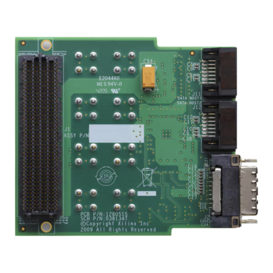
Figure 1-2 shows a block diagram of the XM104. Each MGT data port interface consists of two differential pairs of MGT signals, one pair for the transmitter and one pair for the receiver. MGT Data Ports 0 and 1 are each wired to four SMA connectors. MGT Data Ports 2 and 3 are each wired to host Serial ATA connectors J11 and J12 respectively. -
Page 11: Detailed Description
Figure 1-3 correlate to the features and notes listed in Table 1-2, page 12. For full functionality, the XM104 must be installed on a board FMC connector supporting high pin count interfaces. X-Ref Target - Figure 1-3 UG536_03_111609 Figure 1-3: XM104 Features FMC XM104 Connectivity Card User Guide www.xilinx.com... - Page 12 J11. The connector is mounted on the bottom side of the Serial ATA Port 1 XM104. This connector is mounted on the bottom side of the card. FPGA multi-gigabit transceiver data port 3 on Serial ATA host MGT Data Port 3: connector J12.
-
Page 13: Vita 57.1 Fmc Hpc Connector J1
The XM104 uses Samtec FMC HPC connector part number ASP-134488-01. The XM104 connector mates with an FMC connector. See Xilinx board user guides and schematics for a description of features provided by HPC interfaces contained on the board, including power supply specifications, FPGA banking connectivity, and FPGA pin assignments. -
Page 14: Multi-Gigabit Transceiver Data Port 2 - J11 Sata1
5. Multi-Gigabit Transceiver Data Port 3 - J12 SATA2 Board FPGA multi-gigabit transceiver Data Port 3 signals are wired to a Serial ATA host connector J12 on the XM104. Data Port 3 connections on the XM104 FMC HPC connector and Serial ATA connector J12 are defined in Table 1-6. -
Page 15: Multi-Gigabit Transceiver Data Ports [4:7] - J2 10Ge Base-Cx4 Connector
Board FPGA multi-gigabit transceiver Data Ports 4 through 7 are wired to a 10GE Base- CX4 connector J2 on the XM104. The four data port connections between the XM104 FMC HPC connector and the 10G Base-CX4 connector J2 are defined in Table 1-7. -
Page 16: Pca9543 Iic Switch
The IIC address of this component is controlled by a combination of the board interface and chip enable connections to the component inputs on the XM104. Signals GA0 and GA1 from the board are connected to the two address inputs A1 and A0 of the PCA9543 component. - Page 17 The two downstream IIC devices connected to the PCA9543 are at the following IIC addresses: • Si570 IIC address is at 0x5D • Si5368 IIC address is at 0x68 FMC XM104 Connectivity Card User Guide www.xilinx.com UG536 (v1.1) September 24, 2010 Downloaded from Elcodis.com electronic components distributor...
-
Page 18: Clocking Circuits
Si5368 differential clock inputs. The default clock frequency is 156.25 MHz. Connections to the FMC HPC connector are defined in Table 1-11. Table 1-11: Si570 Clock Source Routed to XM104 FMC HPC J1 Connector FMC HPC Connector J1 Signal Name Source... -
Page 19: Silicon Labs Si5368
Board Technical Description Silicon Labs Si5368 A Silicon Labs Si5368 any-rate precision clock multiplier/jitter attenuator integrated circuit provides a wide range of clocking applications for the Xilinx board and XM104 combination. Table 1-13 shows the connections of the SI5368 differential clock outputs to the XM104 FMC HPC connector. - Page 20 The Si5368 is located at IIC address 0x68. For additional application information on the Si5368 component see the manufacturer's data sheet at www.silabs.com. www.xilinx.com FMC XM104 Connectivity Card User Guide UG536 (v1.1) September 24, 2010 Downloaded from Elcodis.com electronic components distributor...
Need help?
Do you have a question about the XM104 and is the answer not in the manual?
Questions and answers