Table of Contents
Advertisement
Quick Links
Quick Start ADC1002S020
Demonstration board for ADC1002S020
Rev. 2 — 11 octobre 2010
Document information
Info
Content
Keywords
DEMO8766G, PCB769-2, Demonstration board, ADC, Converter,
ADC1002S020
Abstract
This document describes how to use the demonstration board
DEMO8766G for the analog-to-digital converter ADC1002S020.
Overview
Quick Start
Advertisement
Table of Contents

Subscribe to Our Youtube Channel
Related Manuals for NXP Semiconductors ADC1002S020


Summary of Contents for NXP Semiconductors ADC1002S020
- Page 1 Demonstration board for ADC1002S020 Rev. 2 — 11 octobre 2010 Quick Start Document information Info Content Keywords DEMO8766G, PCB769-2, Demonstration board, ADC, Converter, ADC1002S020 Abstract This document describes how to use the demonstration board DEMO8766G for the analog-to-digital converter ADC1002S020. Overview...
- Page 2 Quick Start ADC1002S020 NXP Semiconductors QS ADC1002S020 Revision history Date Description 20080612 Initial version. 20101011 Update for data acquisition system. Contact information For additional information, please visit: http://www.nxp.com For sales office addresses, please send an email to: salesaddresses@nxp.com QS_ADC1002S020_2 All information provided in this document is subject to legal disclaimers.
-
Page 3: Overview Of The Adc1002S020 Demo Board
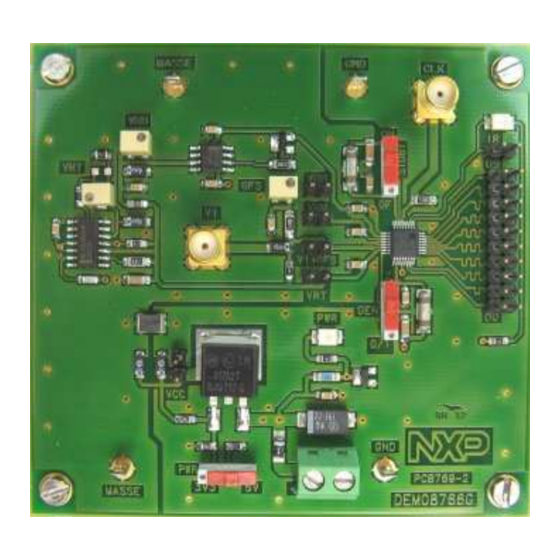
1. Overview of the ADC1002S020 demo board 1.1 ADC1002S020 demoboard Figure 1 presents the connections to measure the ADC1002S020 based on DEMO8766G: SYNTHESIZED Synchronized SIGNAL GENERATOR LOCK SIGNAL . sinewave . AC SYNTHESIZED SIGNAL LOGIC ANALYZER GENERATOR Output data: NPUT SIGNAL . -
Page 4: Power Supply
GND test point – Digital ground STDBY switch – ADC stand-by activation ADC active ADC OFF 1.3 DC voltage adjustments The ADC1002S020 allows to adjust the full scale input signal from 1.6 V to 2.4 V. Table 2. DC voltage adjustments Name Function View VRT trimmer –... -
Page 5: Input Signals (Vi, Clk)
Quick Start ADC1002S020 NXP Semiconductors QS ADC1002S020 1.4 Input signals (VI, CLK) To ensure a good evaluation of the device, the input signal and the input clock must be synchronized together. Moreover, the input frequency (Fi, MHz) and the clock frequency (Fclk, Msps) should follow the formula: , where M is an odd number of period and N is the number of samples. -
Page 6: Hsdc Extension Module: Acquisition Board
2. HSDC extension module: acquisition board figure 2 shows an overview of the extension module HSDC-EXTMOD01/DB acquisition board: +5V P OWER SUPPLY . I = 3.2 A UMPER FOR SUPPLY . define either I/O is 1.8 V or 3.3 V SIGNAL GENERATOR EFERENCE SIGNAL... -
Page 7: Hsdc Extension Module: Hardware Initialization7
• 16-bit LVDS DDR input data stream up to 320 MHz; • On-board or external reference for signal generation. In this section the specific requirement for the use with ADC1002S020 demo-board will be shown. For more details on the HSDC-EXTMOD01/DB, please contact dataconverter- support@nxp.com. -
Page 8: Hsdc Extension Module: Cmos Connector Description
Quick Start ADC1002S020 NXP Semiconductors QS ADC1002S020 Fig 4. “USBConfigSetup” window: step 2 Click “Next” to continue: Fig 5. “USBConfigSetup” window: step 3 Click “Next” to finish the installation process. The system is now ready to use the ADC1412D series board for evaluation purpose. - Page 9 Quick Start ADC1002S020 NXP Semiconductors QS ADC1002S020 Fig 6. HSDC extension module: HE14 CMOS hardware schematic overview The HSDC extension module can acquire data in CMOS level using: • either the on-board clock generated by the internal PLL, refer to as pDFS_CLK[0]/nDFS_CLK[0] that will be used by the FPGA.
- Page 10 Quick Start ADC1002S020 NXP Semiconductors QS ADC1002S020 • or the clock provided by the ADC refer to as P1_CLK_IN. This is the preferred situation since the user will not deal with any set-up/hold timing for the acquisition. Refer to section 3.2 for software configuration.
-
Page 11: Combo Adc1002S020 And Hsdc Extension Module
3.1 Measurement set-up overview figure 07 below shows an overview of the whole system ADC1002S020+HSDC extension module for which connection is done with the accessory (HSDC-ACC07/DB). The measurement set-up presented below shows 1 generator for input signal. Clock signal is delivered by the... -
Page 12: Hsdc Extension Module: Fpga Flash
Quick Start ADC1002S020 NXP Semiconductors QS ADC1002S020 3.2 HSDC extension module: FPGA flash To get access to the software control of the generation system, run the “USB Configurator.exe”. It is located by default in the directory "C:\Program Files\Electronique Concept\USB Configurator\". -
Page 13: Hsdc Extension Module: Pattern Acquisition
Select one-shot mode and source P1 to acquire data (see figure 10). The hardware connection between the ADC1002S020 and the HSDC extension module has to be described to get correct results. This is done by using the fields in “Channel 0 Input Configuration” and in “Channel 1 Input Configuration”. -
Page 14: Pattern Acquisition
Quick Start ADC1002S020 NXP Semiconductors QS ADC1002S020 Fig 10. “USB Configurator” window: pattern acquisition for ADC1002S020 3.4.1 Pattern acquisition Browse on both channel path configuration to select the file to store the data that will be acquired. Click on “Acquire” and “Save” buttons to end the capture process. -
Page 15: Acquisition Software: Input Files
Quick Start ADC1002S020 NXP Semiconductors QS ADC1002S020 Fig 11. “NXP_ADC_Acquisition” window: start-up screen 3.5.1 Acquisition software: input files The first step consists in delivering the files to be processed. Browse in field “Select ADC1 file:” to indicate the file to be used. -
Page 16: Acquisition Software: Fft Results Display
Quick Start ADC1002S020 NXP Semiconductors QS ADC1002S020 Fig 12. “NXP_ADC_Acquisition” window: frequency entry 3.5.3 Acquisition software: FFT results display Press the “COMPUTE” button to display the results from the FFT processing. The results fields will be updated depending on the number of input files. If 2 files have been processed, it is possible to display both results on the same picture for all graphs using the “Display …”... -
Page 17: Reorganized Signal
Quick Start ADC1002S020 NXP Semiconductors QS ADC1002S020 Fig 13. “NXP_ADC_Acquisition” window: FFT result Press the “Autoscale” button to display the whole content. The tables give the relevant dynamic parameters: • Table : first 6 harmonics frequencies and amplitude level; • Table : dynamics parameters: −... -
Page 18: Unreconstruted Signal
Quick Start ADC1002S020 NXP Semiconductors QS ADC1002S020 Fig 14. “NXP_ADC_Acquisition” window: reorganized signal Press the “Autoscale” button to display the whole content. 3.5.3.3 Unreconstruted signal The unreconstructed signal displays the unreconstructed sine wave corresponding to the whole number of period being acquired following the coherency rule: QS_ADC1002S020_2 All information provided in this document is subject to legal disclaimers. -
Page 19: Histogram
Quick Start ADC1002S020 NXP Semiconductors QS ADC1002S020 Zoom tool Fig 15. “NXP_ADC_Acquisition” window: unreconstruted signal Press the “Autoscale” button to display the whole content. Use the zoom tool to observe in more details all the captured data. 3.5.3.4 Histogram The histogram graph shows the distribution of output codes. This graph allows to know... - Page 20 Quick Start ADC1002S020 NXP Semiconductors QS ADC1002S020 Fig 16. “NXP_ADC_Acquisition” window: code histogram Press the “Autoscale” button to display the whole content. The table shows the range of output codes. QS_ADC1002S020_2 All information provided in this document is subject to legal disclaimers.
-
Page 21: Appendix A.1: Coherency Calculation
Quick Start ADC1002S020 NXP Semiconductors QS ADC1002S020 4. Appendix A.1: coherency calculation The coherency relies on the fact that clock and analog input signal are synchronized and the first and last samples being captured are adjoining samples: it ensures a continuous digitized time process for the FFT processing. -
Page 22: Notes
Quick Start ADC1002S020 NXP Semiconductors QS ADC1002S020 5. Notes For any question, feel free to contact us at the following e-mail dataconverter- support@nxp.com. QS_ADC1002S020_2 All information provided in this document is subject to legal disclaimers. © NXP B.V. 2010. All rights reserved. -
Page 23: Legal Information
However, NXP Semiconductors does not give any representations or warranties, expressed or implied, as to the accuracy or In no event shall NXP Semiconductors, its affiliates or their suppliers be completeness of such information and shall have no liability for the liable to customer for any special, indirect, consequential, punitive or consequences of use of such information. -
Page 24: Table Of Contents
Quick Start ADC1002S020 NXP Semiconductors QS ADC1002S020 7. Contents Overview of the ADC1002S020 demo board ..3 ADC1002S020 demoboard ........3 Power supply............4 DC voltage adjustments ........4 Input signals (VI, CLK) ........5 Output signals (D0 to D9, IR) ......5 HSDC extension module: acquisition board..6 HSDC extension module: hardware initialization7 HSDC extension module: software initialization .7...
Need help?
Do you have a question about the ADC1002S020 and is the answer not in the manual?
Questions and answers