NXP Semiconductors LPCXpresso55S69 User Manual
Hide thumbs
Also See for LPCXpresso55S69:
- User manual (24 pages) ,
- User manual (20 pages) ,
- User manual (28 pages)
Table of Contents
Advertisement
Quick Links
Advertisement
Table of Contents

Related Manuals for NXP Semiconductors LPCXpresso55S69


Summary of Contents for NXP Semiconductors LPCXpresso55S69
- Page 1 UM11158 LPCXpresso55S69/55S28 Development Boards Rev. 1.6 — 17 March 2022 User manual Document information Info Content Keywords LPC55S69, LPC55S6x, LPCXpresso55S69, LPC55S69-EVK, LPC55S28, LPCXpresso55S28, LPC55S28-EVK Abstract LPCXpresso55S69/55S28 user manual...
- Page 2 UM11158 NXP Semiconductors LPCXpresso55S69/55S28 Development Boards Revision history Date Description • 20220317 Section 10 “Errata” added title Section 10.1 “Brown-out detect (BOD) may be triggered during boot (code execution from ROM)”. • Added Section 10.2 “SPI ISP mode” Section 10.3 “Power supply rise time”.
-
Page 3: Introduction
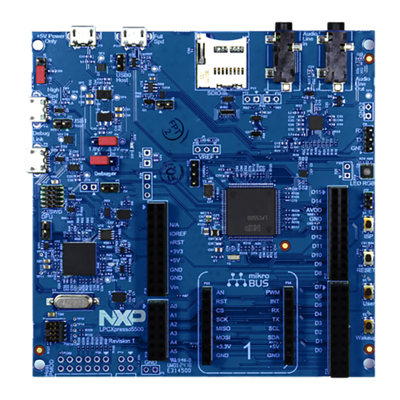
Fig 1. LPCXpresso55S69 The LPCXpresso55S69 and LPCXpresso55S28 boards include the following features: • LPC55S69 Dual Cortex-M33 core processor or LPC55S28 Cortex-M33 processor UM11158 All information provided in this document is subject to legal disclaimers. - Page 4 UM11158 NXP Semiconductors LPCXpresso55S69/55S28 Development Boards • Onboard, high-speed USB, Link2 debug probe with CMSIS-DAP and SEGGER J-Link protocol options • UART and SPI port bridging from LPC55Sxx target to USB via the onboard debug probe • Optional external debug probes with trace option (10 or 20 pin Cortex-M connectors) •...
-
Page 5: Board Layout And Settings
UM11158 NXP Semiconductors LPCXpresso55S69/55S28 Development Boards 2. Board layout and Settings Figure 2 shows the layout of the board (top side), indicating location of the connectors and buttons, while Figure 3 shows locations of jumpers and headers. Table 1 provides a description of connectors, jumpers, LEDs and buttons. - Page 6 UM11158 NXP Semiconductors LPCXpresso55S69/55S28 Development Boards Fig 3. Board jumpers and headers Table 1. Indicators, buttons, connectors and LEDs Circuit Description Default Reference reference Target power indicator LED Link2 boot LED Section 4.1 RGB User LED Section 7.4 Audio codec line input jack Section 7.1...
- Page 7 UM11158 NXP Semiconductors LPCXpresso55S69/55S28 Development Boards Table 1. Indicators, buttons, connectors and LEDs Circuit Description Default Reference reference Target processor selection for the on-board Debug Probe. Not installed Section 4. Jumper open (default) the LPC55Sxx Target SWD interface enabled. Normal operating mode where the Target SWD is connected to either the on-board Link2 Debug Probe or an external Debug Probe.
- Page 8 UM11158 NXP Semiconductors LPCXpresso55S69/55S28 Development Boards Table 1. Indicators, buttons, connectors and LEDs Circuit Description Default Reference reference Serial port header Section 6.2 0.1” header providing convenient access to Flexcom 0 USART (the USART used for ISP boot). When using this port install jumper P1 to disable the Link2 connection to this port.
-
Page 9: Getting Started
UM11158 NXP Semiconductors LPCXpresso55S69/55S28 Development Boards Table 1. Indicators, buttons, connectors and LEDs Circuit Description Default Reference reference ISP/User button Section 7.5.1 When pressed, this button connect sport pin P0_5 to ground. Hold this button down while pressing and releasing Reset (S4) to force the LPC55Sxx into ISP mode. -
Page 10: Starting A Debug Session Using The On-Board (Link2) Debug Probe
Connect the board to the USB port of your host computer, connecting a micro USB cable to connector P6. The board will boot and run the pre-installed demo. Allow about 10 seconds for the LPCXpresso55S69/S28 Board to enumerate for the first time; the device will appear as "LPC Device". -
Page 11: Installation Steps To Use Keil And Iar Tools With On-Board Debug Probe
UM11158 NXP Semiconductors LPCXpresso55S69/55S28 Development Boards 3.2.2 Installation steps to use Keil and IAR tools with on-board debug probe Download and install LPCScrypt (https://www.nxp.com/lpcscrypt). This will install required drivers for the board. Note that the Link2 (LPC4322 device) is pre-programmed with CMSIS-DAP firmware. -
Page 12: On-Board (Link2) Debug Probe
VCOM port can be used if the board is running an application when no debugger is running. In order to correctly install and use the Link2 device on the LPCXpresso55S69 (required for any debugging purpose) for Windows 7 or 8 host computers, install the drivers first. -
Page 13: Link2 Boot Led
The Link2 Debug Probe SWD should be connected by a ribbon cable between the P1 connector to the off-board target MCU SWD interface. Power the LPCXpresso55S69 board from the Link USB connector P6, and fit jumper J3 across pins 2 - 3 (External Target). -
Page 14: Board Power
LPCXpresso55S69/55S28 Development Boards 5. Board Power The LPCXpresso55S69 board requires +5V input to power the on-board voltage low dropout linear regulators, of which there are 3, all available from Torex Semiconductor. The Link2 Debug probe has a 2.5V regulator (U10) which draws power from USB connector P6 (“Debug Link”) only. -
Page 15: Measuring Lpc55Sxx Device Supply Current
The Board incorporates micro AB connectors for both of USB0 (Full Speed, connector P10) and USB1 (High Speed, connector P9) ports of the LPCXpresso55S69. Both of these ports are capable of operating as a device or a host, and this is why micro AB connectors are used. -
Page 16: On-Board Peripherals
Codec. See schematic for further information. 7.2 Micro SD card slot The micro SD card (P21) included in the LPCXpresso55S69 board provides a 4-bit SDIO interface to support memory cards, plug-in WiFi modules, etc. Power enable to the socket is provided via transistor enabled by P1_0. -
Page 17: Accelerometer
P18. 7.5 Buttons Four buttons are provided on the LPCXpresso55S69, as described in this section. 7.5.1 ISP (S1) P0_5 is pulled up to VDD via a 2.2 kohm resistor; pressing this button will pull P0_5 low. -
Page 18: User (S3) And Wake (S2) Buttons
LPC55S6x/LPC55S2x/LPC552x User manual for further information. 8. Expansion connectors The LPCXpresso55S69 includes 3 expansion connector sets, incorporating support for Arduino UNO R3, Mikroe Click and PMod standards. The Arduino UNO connector footprint is surrounded by additional connectors that are compatible with other LPCXpresso V3 boards. -
Page 19: Arduino And Lpcxpresso V3 Expansion Connectors
Mikroe Click site, audio codec and RGB LED. Refer to the schematic for further information. When using an Arduino shield with the Board, align P17 of the Arduino shield (SCL) with pin 1 of connector P17 on the LPCXpresso55S69 board. Table 5. Micro SD card connections... - Page 20 UM11158 NXP Semiconductors LPCXpresso55S69/55S28 Development Boards Fig 4. P16 and P19 connector pinouts Fig 5. P17 and P18 connector pinouts UM11158 All information provided in this document is subject to legal disclaimers. © NXP B.V. 2022. All rights reserved. User manual Rev.
-
Page 21: Other Features
10.1 Brown-out detect (BOD) may be triggered during boot (code execution from ROM) Initial production LPCXpresso55S69 boards, marked as Revision A1, use LPC55S69 revision 0A silicon. Please refer to errata documentation from NXP for full details of device errata (https://www.nxp.com/docs/en/errata/ES_LPC55S6x.pdf). -
Page 22: Power Supply Rise Time
UM11158 NXP Semiconductors LPCXpresso55S69/55S28 Development Boards 10.3 Power supply rise time The minimum rise time of the power supply on the LPC55S69/S28 does not meet the power-up ramp conditions specified in the datasheet. Please see the data sheet and VBAT_DCDC.1 errata in the errata sheet. -
Page 23: Table Of Contents
VCOM port ......13 Configuring the LPCXpresso55S69 to debug an off-board target ......13 Board Power. - Page 24 Right to make changes - NXP Semiconductors reserves the right to make changes to information published in this document, including without limitation specifications and product descriptions, at any time and without notice.
- Page 25 and service marks licensed by Power.org. M, M Mobileye and other Mobileye trademarks or logos appearing herein are trademarks of Mobileye Vision Technologies Ltd. in the United States, the EU and/or other jurisdictions. © NXP B.V. 2018-2022. All rights reserved. For more information, please visit: http://www.nxp.com For sales office addresses, please send an email to: salesaddresses@nxp.com Date of release: 17 March 2022...
Need help?
Do you have a question about the LPCXpresso55S69 and is the answer not in the manual?
Questions and answers