
Related Manuals for iWave iW-RainboW-G27D


Summary of Contents for iWave iW-RainboW-G27D
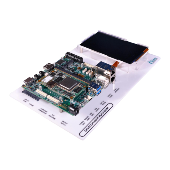
- Page 1 8 QM/QP Qseven Development Platform Hardware User Guide iW-RainboW-G27D i.MX8 QuadMax/QuadPlus Qseven Development Platform Hardware User Guide REL1.0 iWave Systems Technologies Pvt. Ltd. Page 1 of 81...
- Page 2 If you are not the intended recipient (or authorized to receive for the recipient), you are hereby notified that any disclosure, copying distribution or use of any of the information contained within this document is STRICTLY PROHIBITED. Thank you. “iWave Systems Tech. Pvt. Ltd.” REL1.0 iWave Systems Technologies Pvt.
- Page 3 No warranty of accuracy is given concerning the contents of the information contained in this publication. To the extent permitted by law no liability (including liability to any person by reason of negligence) will be accepted by iWave Systems, its subsidiaries or employees for any direct or indirect loss or damage caused by omissions from or inaccuracies in this document.
-
Page 4: Table Of Contents
2.8.5 USB2.0 Header ............................58 ............................59 OARD WITCHES 2.9.1 Power ON/OFF Switch ..........................59 2.9.2 Reset Switch ..............................60 2.9.3 Board Configuration Switch ........................61 SOM E ..........................63 XPANSION ONNECTORS REL1.0 iWave Systems Technologies Pvt. Ltd. Page 4 of 81... - Page 5 ..........................77 ECHANICAL HARACTERISTICS 3.4.1 i.MX 8 QM/QP Qseven Carrier Board Mechanical Dimensions ..............77 3.4.2 Guidelines to insert the Qseven SOM into Carrier Board ................79 ORDERING INFORMATION .......................... 80 REL1.0 iWave Systems Technologies Pvt. Ltd. Page 5 of 81...
- Page 6 ECHANICAL DIMENSIONS OF I SEVEN ARRIER OARD OTTOM 31: M .MX 8 QM/QP Q ..........79 IGURE ECHANICAL DIMENSIONS OF I SEVEN ARRIER OARD 32: SOM I ............................79 IGURE NSERTION UIDELINE REL1.0 iWave Systems Technologies Pvt. Ltd. Page 6 of 81...
- Page 7 17: P ............................75 ABLE OWER NPUT EQUIREMENT 18: P ............................75 ABLE OWER UTPUT PECIFICATION 19: E ............................ 76 ABLE NVIRONMENTAL PECIFICATION 20: O ........................... 80 ABLE RDERABLE RODUCT UMBERS REL1.0 iWave Systems Technologies Pvt. Ltd. Page 7 of 81...
-
Page 8: Introduction
This document is the Hardware User Guide for the i.MX 8 QM/QP Qseven V2.1 Development platform “iW-RainboW- G27D” based on the NXP’s i.MX8 Application processor. This board is fully supported by iWave Systems Technologies Pvt. Ltd. This Guide provides detailed information on the overall design and usage of the i.MX 8 QM/QP based Qseven development platform from a Hardware Systems perspective. - Page 9 Real Time Clock SATA Serial Advanced Technology Attachment Secure Digital System On Module To Be Defined UART Universal Asynchronous Receiver/Transmitter Universal Serial Bus USB OTG USB On The Go Voltage REL1.0 iWave Systems Technologies Pvt. Ltd. Page 9 of 81...
-
Page 10: Terminology Description
Note: Signal Type does not include internal pull-ups or pull-downs implemented by the chip vendors and only includes the pull-ups or pull-downs implemented On- Qseven SOM. References • IMX8QMAEC_Revx.pdf • iMX8QM_RM_Rev_x.pdf • Qseven® Specification Version 2.1 • Qseven® Design Guide 2.0 REL1.0 iWave Systems Technologies Pvt. Ltd. Page 10 of 81... -
Page 11: Architecture And Design
This section provides detailed information about the i.MX 8 QM/QP Qseven SOM features and Hardware architecture with high level block diagram. I .MX 8 QM/QP Qseven Development Platform Block Diagram Figure 1: i.MX 8 QM/QP Qseven Development Platform Block Diagram REL1.0 iWave Systems Technologies Pvt. Ltd. Page 11 of 81... -
Page 12: I.mx 8 Qm/Qp Qseven Development Platform Features
• RTC Coin Cell holder • Buzzer • Fan Header • 20 - Pin JTAG Header On Board Switches • Power ON/OFF Switch • Board Configuration Switch • Reset Switch REL1.0 iWave Systems Technologies Pvt. Ltd. Page 12 of 81... - Page 13 : 120mm X 120mm Nano ITX Either USB 2.0 in Mini PCIe connector or USB 3.0 Type A TOP connector can be supported at a time. Anyone can be selected using on Board Switches. REL1.0 iWave Systems Technologies Pvt. Ltd. Page 13 of 81...
-
Page 14: Qseven Mxm Connector
This standard 230-pin robust connector is capable of handling high-speed serialized signals and can be used for size constrained embedded applications. This Qseven MXM connector (J13) is physically located at the top of the board as shown below. Figure 2: Qseven MXM Connector REL1.0 iWave Systems Technologies Pvt. Ltd. Page 14 of 81... -
Page 15: Qseven Pcb Edge Connector Pin Assignment
(SW5) in carrier board. SUS_S3# SUS_S3_Q7 I, 3.3V S3 state. CMOS/10K PU This pin is connected to indication LED D13. SUS_STAT# SUS_STAT_Q7(GPI ESAI1_FST/ I, 3.3V Suspend Status. O2_05) BF12 CMOS/10K PU REL1.0 iWave Systems Technologies Pvt. Ltd. Page 15 of 81... - Page 16 This pin connected to M.2 SATA TX0_N/ C17 Connector (J33) for SATA Channel0 Transmit differential pair negative. SATA1_TX- NC in i.MX8 Qseven SOM. This pin connected to 7pin SATA Connector (J20) in carrier board. (Optional) REL1.0 iWave Systems Technologies Pvt. Ltd. Page 16 of 81...
- Page 17 IO1_23) This pin is connected from SD/MMC /BK24 connector(J28)/Optionally Connected With (J27) Micro Sd SDIO_LED GPIO_SD1_LED(GPI SPI0_CS1/ I, 3.3V CMOS This pin is connected to Power I/O O3_06) Header (J3) REL1.0 iWave Systems Technologies Pvt. Ltd. Page 17 of 81...
- Page 18 NC in i.MX8 Qseven SOM. This pin is connected to SD/MMC connector (J28) in carrier board. RSVD5/SDIO_D NC in i.MX8 Qseven SOM. This pin is connected to SD/MMC connector (J28) in carrier board. REL1.0 iWave Systems Technologies Pvt. Ltd. Page 18 of 81...
- Page 19 THRM# I, 3.3V CMOS This pin is connected from Push button (SW6) in carrier board. WDTRIG# Q7_WDTRIG_B I, 3.3V CMOS This pin is connected to Power I/O Header (J3) 11 REL1.0 iWave Systems Technologies Pvt. Ltd. Page 19 of 81...
- Page 20 This pin is connected to USB3.0 Host Port1 Over current indicator in carrier board. USB_P5- / USB3_HUB3_TXM I, USB SS This pin is connected to USB Switch USB_SSTX2- For M.2 Sata ,Optionally Connected With M.2 PCIe REL1.0 iWave Systems Technologies Pvt. Ltd. Page 20 of 81...
- Page 21 This pin is connected from Micro USB OTG connector (J1).(Optional) USB_P1- USB_OTG1_DM USB_OTG1_D IO, DIFF USB 2.0 OTG Port1 Data negative. This pin is connected to Micro USB OTG connector (J1). REL1.0 iWave Systems Technologies Pvt. Ltd. Page 21 of 81...
- Page 22 LVDS primary channel differential TX1_P/ LVDS_A1+ pair1 positive. BM38 This pin is connected to LVDS Receiver. eDP1_TX1+/ LVDS1_CH1_TX1_P LVDS1_CH1_ LVDS, DIFF LVDS secondary channel differential TX1_P/ LVDS_B1+ pair1 positive. BM32 REL1.0 iWave Systems Technologies Pvt. Ltd. Page 22 of 81...
- Page 23 LVDS, DIFF LVDS primary channel differential TX3_P/ LVDS_A3+ pair3 positive. BM40 This pin is connected to LVDS Receiver. eDP1_TX3+/ LVDS1_CH1_TX3_P LVDS1_CH1_ LVDS, DIFF LVDS secondary channel differential TX3_P/ LVDS_B3+ pair3 positive. REL1.0 iWave Systems Technologies Pvt. Ltd. Page 23 of 81...
- Page 24 10K PU Control. BD34 GP_1-Wire_Bus HDMI_TX0_CEC HDMI_TX0_C O, 3.3V CMOS This pin is connected to HDMI connector (J25) in carrier board. GP2_I2C_DAT/L LVDS1_I2C0_SDA LVDS1_I2C0_ IO, 3.3V OD/ I2C3 Data. SDA/E33 VDS_DID_DAT REL1.0 iWave Systems Technologies Pvt. Ltd. Page 24 of 81...
- Page 25 Ground. Power Ground. DP_LANE1+/ HDMI_TX0_DATA1 HDMI_TX0_D I, HDMI or EDP HDMI differential data lane 1 ATA1_EDP1_ positive. TMDS_LANE1+ _P/EDP1_P P /BL7 This pin is connected to Switch For DP/HDMI Function REL1.0 iWave Systems Technologies Pvt. Ltd. Page 25 of 81...
- Page 26 (J25) in carrier board. DP_LANE0-/ HDMI_TX0_DATA2 HDMI_TX0_D I, HDMI or EDP HDMI differential data lane 2 ATA2_EDP0_ TMDS_LANE2- _N/EDP0_N negative. N /BM8 This pin is connected to Switch For DP/HDMI Function. REL1.0 iWave Systems Technologies Pvt. Ltd. Page 26 of 81...
- Page 27 This pin is connected to M.2 Pcie(J31).(Optional) PCIE3_RX- NC in i.MX8 Qseven SOM. This pin is connected to M.2 Pcie(J31).(Optional) Power Ground. Power Ground. PCIE2_TX+ NC in i.MX8 Qseven SOM. REL1.0 iWave Systems Technologies Pvt. Ltd. Page 27 of 81...
- Page 28 This pin is connected from Data UART Header (J6) 02 Pin. PCIE0_TX+ PCIE0_A_TX0_P PCIE0_TX0_P I, DIFF PCIe Channel0 Transmit data output /B26 positive. This pin is connected to M.2 PCIe connector (J31) in carrier board. REL1.0 iWave Systems Technologies Pvt. Ltd. Page 28 of 81...
- Page 29 _00) 10K PU LVDS LCD Panel Power Enable. 192 LPC_LDRQ#/ Q7_GPIO_7(GPIO0 LSIO.GPIO0.I IO, 3.3V CMOS M.2 Host Wake Connected With M.2 O00/AL45 GPIO7 _00) SATA Optionally Connected With M.2 PCIe REL1.0 iWave Systems Technologies Pvt. Ltd. Page 29 of 81...
- Page 30 This pin is connected to 5V standby power supply in carrier board. 206 VCC_5V_SB2 NC in i.MX8 Qseven SOM. This pin is connected to 5V standby power supply in carrier board. REL1.0 iWave Systems Technologies Pvt. Ltd. Page 30 of 81...
- Page 31 VCC_5V O, 5V Power Supply Voltage. 228 VCC VCC_5V O, 5V Power Supply Voltage. 229 VCC VCC_5V O, 5V Power Supply Voltage. 230 VCC VCC_5V O, 5V Power Supply Voltage. REL1.0 iWave Systems Technologies Pvt. Ltd. Page 31 of 81...
-
Page 32: Serial Interface Features
Micro AB Connector (J2). This USB Micro AB Connector can be used for Debug purpose which is physically located at the top of the board as shown below. Figure 3: Debug UART Port REL1.0 iWave Systems Technologies Pvt. Ltd. Page 32 of 81... -
Page 33: Data Uart Interface
3.3V Supply Voltage. (optional) UART0_RXD I, 3.3V CMOS UART0 interface Receive signal. UART0_TXD O, 3.3V CMOS UART0 interface Transmit signal. RTS# UART0_CTS#s I, 3.3V CMOS UART0 interface Ready to Send signal. REL1.0 iWave Systems Technologies Pvt. Ltd. Page 33 of 81... -
Page 34: High Speed Interface Features
O, 3.3V CMOS M.2 Wireless Disable Signal 10K PU GND2 USBP3- IO, USB USB2.0 Port3 Data Minus. DAS/DSS GPIO_SATA_ACT#(GPIO1_1 O, 3.3V CMOS Provide status indicators via LED.(D9) Note: GPIO1_18 Connected Optionally. REL1.0 iWave Systems Technologies Pvt. Ltd. Page 34 of 81... - Page 35 I/O 1.8V CMOS General Purpose input Output GND7 Power Ground N/A15 SATA-A-/PETn0 PCIE_SATA0_TX0_N I, PCIe PCIe Channel A/B Receive Positive N/A16 SATA-A+/PETp0 PCIE_SATA0_TX0_P I, PCIe PCIe Channel A/B Receive Positive PERST# GND8 Power Ground REL1.0 iWave Systems Technologies Pvt. Ltd. Page 35 of 81...
-
Page 36: Sata Interface
M.2 SATA connector (J33). The Qseven carrier board also supports SATA activity LED (D17) on Top side of the board for SATA activity indication. This M.2 SATA Connecter is physically located at the top of the board. REL1.0 iWave Systems Technologies Pvt. Ltd. Page 36 of 81... -
Page 37: Figure 6: M.2 Sata Connector
O, 3.3V CMOS M.2 Wireless Disable Signal (O)(0/3.3V) USB_D- USB_HUB3OUT_DM IO, USB USB2.0 Host Port3 Data Minus. GPIO9(LED1#/DAS_D O, 3.3V CMOS Provide status indicators via LED M.2_LED_1 SS#)(I)(0/3.3V) Power Ground. REL1.0 iWave Systems Technologies Pvt. Ltd. Page 37 of 81... - Page 38 SIM Card Power. PETP1/USB3.1- USB 3.0 Transferring Data Positive TX+/SSIC-TXP DEVSLP (O) Power Ground. GPIO0(SMB_CLK/GN DMA_I2C1_SCL O, 1.8V CMOS I2C CLK. SS_SCL/SIM_DET2)(I/ O)(0/1.8V) PERN0/SATA_B+ PCIE_SATA0_RX0_P I,PCIe/SATA PCIe Port 0 Receive Lane Positive. REL1.0 iWave Systems Technologies Pvt. Ltd. Page 38 of 81...
- Page 39 UART Receiving signal Is Connected (I)(0/1.8V) ANTCTL3 (I)(0/1.8 V) SIM_DETECT (I) M.2_SIM_DETECT_1 10K PU with This pin is connect With Sim Detect Pin 3.3V RESET# (O)(0/1.8V) Q7_GPIO_5(GPIO1_1 I,O 3.3V CMOS M.2 Reset Signal (OPTIONAL) REL1.0 iWave Systems Technologies Pvt. Ltd. Page 39 of 81...
- Page 40 Ground. VCC_3V3 VCC_3V3 O, 3.3V Power 3.3V Supply Voltage. Power Ground. VCC_3V3 VCC_3V3 O, 3.3V Power 3.3V Supply Voltage. CONFIG_2 M.2_CONFIG_2 I, 3.3V CMOS M.2 Configuration Pin 2. 10K PU REL1.0 iWave Systems Technologies Pvt. Ltd. Page 40 of 81...
-
Page 41: Nano Sim Connecter
SATA (optionally connect with M.2 PCIe) Power Ground Power Ground Optionally Connected with M2_UIM_PWR O, Signal Sim Card data Signal Connect with M.2 Sata SIM_DAT (optionally connect with M.2 PCIe) Power Ground REL1.0 iWave Systems Technologies Pvt. Ltd. Page 41 of 81... -
Page 42: Usb3.0 Host Interface
Qseven MXM connector USB port 6 & 7. This USB3.0 connector (J22) is physically located at the top of the board as shown below. Figure 8: USB3.0 Host REL1.0 iWave Systems Technologies Pvt. Ltd. Page 42 of 81... -
Page 43: Communication Interface Features
RJ45 Magjack (J21). Also, it supports Speed (Yellow) and Link/Activity (Green) LED indications on RJ45 Magjack. This RJ45 Magjack combo connector is physically located at the top of the board as shown below. Figure 9: RJ45 Magjack REL1.0 iWave Systems Technologies Pvt. Ltd. Page 43 of 81... -
Page 44: Usb2.0 Otg Interface
This USB2.0 Port1 signals of Qseven MXM connector is directly connected to USB2.0 Micro AB connector (J1) This USB2.0 OTG connector is physically located at the top of the board as shown below. Figure 10: USB2.0 OTG REL1.0 iWave Systems Technologies Pvt. Ltd. Page 44 of 81... -
Page 45: Sdio Interface
This power enable/disable is controlled from the SDIO_PWR# pin of Qseven MXM connector This SD/MMC connector (J28) is physically located at the bottom of the board as shown below. Figure 11:Standard SD Connector REL1.0 iWave Systems Technologies Pvt. Ltd. Page 45 of 81... -
Page 46: Can Interface
5V Supply Voltage. VCC_12V Note: Optionally connected to 12V supply Voltage. CANL FLEXCAN0_TX IO, DIFF CAN0 Low-Level Voltage I/O Power Ground. CANH FLEXCAN0_RX IO, DIFF CAN0 High-Level Voltage I/O Power Ground. REL1.0 iWave Systems Technologies Pvt. Ltd. Page 46 of 81... -
Page 47: Audio/Video Features
The i.MX 8 QM/QP CPU supports HDMI 2.0 audio/video out. HDMI Signals from the Qseven MXM connector along with HDMI DDC clock & data is connected to Standard HDMI Type-A connector with ESD protection circuitry. Figure 13: HDMI Output REL1.0 iWave Systems Technologies Pvt. Ltd. Page 47 of 81... -
Page 48: Display Port Interface
The i.MX 8 QM/QP CPU supports Display Port (J23) Optional Feature On SOM, the i.MX 8 QM/QP CPU supports Either HDMI or DP. Contact iWave Technical Support team for display port supported SOM. In The Development Platform Through Switch (Refer 2.9.3 Switch) the data lines can shared from HDMI to DP. Display Port (J23) Connecter is physically placed on top. -
Page 49: I2S Audio Interface
Also, Headphone detect and Mic detect is supported through Qseven MXM connector pins GPIO3 (188 Pin) & GPIO2 (187 Pin) correspondingly. These Audio Jacks are physically located at the top of the board as shown below. Figure 15: Audio Jack REL1.0 iWave Systems Technologies Pvt. Ltd. Page 49 of 81... -
Page 50: 7" Lcd With Capacitive Touch
Note: In i.MX 8 QM/QP carrier board, LVDS brightness control GPIO from Qseven MXM connector (123rd Pin) is shared to both primary & secondary LCD’s brightness control. Figure 16: 7” RGB LCD Connector REL1.0 iWave Systems Technologies Pvt. Ltd. Page 50 of 81... -
Page 51: Table 9: 7" Rgb Lcd Connector Pinouts
Display Red Data 2(LSB). VSS9 Power Ground. DCLK DIS_CLK O, 3.3V CMOS DOT Data Clock. HSYNC DIS_HSYNC O, 3.3V CMOS Horizontal SYNC Output. VSYNC DIS_VSYNC O, 3.3V CMOS Vertical SYNC Output. REL1.0 iWave Systems Technologies Pvt. Ltd. Page 51 of 81... -
Page 52: Figure 17: Capacitive Touch Connector
I2C2 Data Signal DMA_I2C2_SDA O,3.3V CMOS /10K PU Touch Controller Reset RST# GPIO_RESET(GPIO1_05) O,3.3V CMOS/10K PU Wake interrupt. WAKE# CAP_WAKE# I,3.3 CMOS/10K PU Touch Controller Interrupt INT# Q7_GPIO_0(GPIO3_12) Power Ground VSS1 REL1.0 iWave Systems Technologies Pvt. Ltd. Page 52 of 81... -
Page 53: Lvds Port With Resistive Touch
I, LVDS LVDS channel differential pair1 positive GND4 Power Ground RIN2- LVDS1_CH1_TX2_N I, LVDS LVDS channel differential pair2 negative RIN2+ LVDS1_CH1_TX2_P I, LVDS LVDS channel differential pair2 positive GND5 Power Ground REL1.0 iWave Systems Technologies Pvt. Ltd. Page 53 of 81... - Page 54 LVDS channel differential Clock positive GND6 Power Ground RIN3- LVDS1_CH1_TX3_N I, LVDS LVDS channel differential pair3 negative RIN3+ LVDS1_CH1_TX3_P I, LVDS LVDS channel differential pair3 positive GND7 Power Ground GND8 Power Ground REL1.0 iWave Systems Technologies Pvt. Ltd. Page 54 of 81...
-
Page 55: Additional Features
) for RTC back up voltage when VCC main power is off. This Coin Cell Holder (J35) is physically located at the top of the board as shown below. Figure 19: RTC Battery Holder REL1.0 iWave Systems Technologies Pvt. Ltd. Page 55 of 81... -
Page 56: Fan Header
O, 12V Power 12V Supply Voltage. PWM3(GPIO0_16) O, 3.3 CMOS Fan Speed control. Power Ground. TACHO FAN_TACHOIN I, 3.3 CMOS Fan tachometer input SPWR VCC_FAN O, Power Fan Power Control. Power Ground. REL1.0 iWave Systems Technologies Pvt. Ltd. Page 56 of 81... -
Page 57: Jtag Header (Optional)
8M/QP Qseven SOM and hence JTAG connector on i.MX 8 QM/QP Qseven carrier board cannot be used for debugging. Number of Pins : 20 Connector Part number : 0015912200 from Molex Mating Connector : 0015445820 from Molex Figure 21: JTAG Header REL1.0 iWave Systems Technologies Pvt. Ltd. Page 57 of 81... -
Page 58: Usb2.0 Header
Table 13: USB2.0 Header Signal Type / Signal Name Description Termination VBUS_HOST_TP Power Supply Voltage 5V USB_HUBOUT3_DM Power USB Data Negative USB_HUBOUT3_DP I, 3.3V CMOS USB Data Positive Power Ground REL1.0 iWave Systems Technologies Pvt. Ltd. Page 58 of 81... -
Page 59: On Board Switches
The i.MX 8 QM/QP Qseven carrier board has power ON/OFF switch (SW1) to control the Main Power Input On/Off functionality. This power ON/OFF switch is physically located at the top of the board as shown below. Figure 23: Power ON/OFF Switch REL1.0 iWave Systems Technologies Pvt. Ltd. Page 59 of 81... -
Page 60: Reset Switch
Qseven MXM connector is directly connected from Reset Push button switch. This Reset Push button switch (SW4) is physically located at the top of the board as shown below. Figure 24: Reset Switch REL1.0 iWave Systems Technologies Pvt. Ltd. Page 60 of 81... -
Page 61: Board Configuration Switch
All the bits of Board configuration switch are not used in i.MX 8 QM/QP Qseven carrier board and so only the required bits are explained with default setting highlighted. REL1.0 iWave Systems Technologies Pvt. Ltd. Page 61 of 81... -
Page 62: Table 14: Board Configuration Switch
MFG4_JTAG_TRST# UART JTAG Configuration Connecter LID_BTN# LID Open LID Close (GPII_0(GPIO3_03) BIOS_DSIABLE# BIOS enable BIOS Disable (ON Som Its Not Connected) (ON Som Its Not Connected) BATLOW# Battery-OK Battery-LOW (GPII_2(GPIO0_05) REL1.0 iWave Systems Technologies Pvt. Ltd. Page 62 of 81... -
Page 63: Som Expansion Connectors
Connectors Part number : DF17(2.0)-80DP-0.5V(57) from Hirose Mating Connector : DF17(3.0)-80DS-0.5V(57) from Hirose Note: For SOM expansion connector pinout, refer the i.MX 8 QM/QP Qseven SOM Hardware User Guide. Figure 26: SOM Expansion Connectors REL1.0 iWave Systems Technologies Pvt. Ltd. Page 63 of 81... -
Page 64: Power And Io Headers
On SOM In this pin is Not Connected VCC_3V3 O,3.3V Power 3.3 V Supply Voltage LVDS_BLC_DAT On SOM In this pin is Not Connected VCC_3V3 Power, O 3.3V Power 3.3V Supply Voltage Power Ground Power Ground REL1.0 iWave Systems Technologies Pvt. Ltd. Page 64 of 81... -
Page 65: Carrier Board Expansion Connectors
QM/QP Qseven SOM Expansion connector 1 & 2 pins, these connectors pinout information are not included in this document. Refer i.MX 8 QM/QP Qseven SOM hardware user guide for Expansion connector 1 & 2 pinout details. REL1.0 iWave Systems Technologies Pvt. Ltd. Page 65 of 81... -
Page 66: Figure 27: Carrier Boarde
I, DIFF MIPI_DSI1 Differential Data Lane 0 Positive _P/BK28 MIPI_DSI1_DATA0_P MIPI_DSI1_DATA0 I, DIFF MIPI_DSI0 Differential Data Lane 0 _P/BG33 Positive MIPI_DSI0_DATA0_N MIPI_DSI0_DATA0 I, DIFF MIPI_DSI0 Differential Data Lane 0 _N/BM28 Negative REL1.0 iWave Systems Technologies Pvt. Ltd. Page 66 of 81... - Page 67 Power Ground HDMI_RX0_CLK_N HDMI_RX0_CLK_N I,DIFF HDMI_RX0 Clock Negative /BL11 MIPI_DSI0_I2C_SDA MIPI_DSI0_I2C_SD I,DIFF MIPI_DSI I2C0 Data A/BE31 HDMI_RX0_CLK_P HDMI_RX0_CLK_P/ I,DIFF HDMI_RX0 Clock Negative BM12 MIPI_DSI0_I2C_SCL MIPI_DSI0_I2C_SC I,DIFF MIPI_DSI I2C0 Clock L/BE29 REL1.0 iWave Systems Technologies Pvt. Ltd. Page 67 of 81...
- Page 68 HDMI_RX0 Differential Data Lane 2 _N/BL19 Negative Power Ground HDMI_RX0_DATA2_P HDMI_RX0_DATA2 I,TDMS HDMI_RX0 Differential Data Lane 2 _P/BM20 Positive ADC_IN4(GPIO3_22) ADC_IN4(GPIO3_2 I, 1.8V CMOS ADC Input 4 2)/AN9 (Note: Optionally UART3_RX) Power Ground REL1.0 iWave Systems Technologies Pvt. Ltd. Page 68 of 81...
- Page 69 ENET1_MDIO ENET1_MDIO/C13 IO,3.3V Management data. CMOS ENET1_RGMII_RXD2 ENET1_RGMII_RXD I, 3.3V CMOS ENET1 receive data2. 2/D52 ENET1_MDC ENET1_MDC/A13 O,3.3V Management data clock. ENET1_RGMII_RXD3 ENET1_RGMII_RXD I, 3.3V CMOS ENET1 receive data3. CMOS REL1.0 iWave Systems Technologies Pvt. Ltd. Page 69 of 81...
-
Page 70: Table 16: Carrier Expansion Connector 1 Pin Out
LVDS0 Channel1 Transmit Lane 2 / BG39 negative. LVDS0_CH0_TX2_P LVDS0_CH0_TX2_P O, LVDS LVDS0 Channel0 Transmit Lane 2 / BM44 positive. LVDS0_CH1_TX2_P LVDS0_CH1_TX2_P O, LVDS LVDS0 Channel1 Transmit Lane 2 / BH40 positive. REL1.0 iWave Systems Technologies Pvt. Ltd. Page 70 of 81... - Page 71 Note: Optionally connected to CMOS VDD_SNVS Power Ground MLB_DATA MLB_DATA/ IO,1.8V Media Local Bus Data. CMOS MLB_DATA_P MLB_DATA_P/ IO, MLB Media Local Bus DATA positive. MLB_CLK MLB_CLK/ O,1.8V Media Local Bus Clock. CMOS REL1.0 iWave Systems Technologies Pvt. Ltd. Page 71 of 81...
- Page 72 SPI2 Clock CMOS/ 33E Series QSPI1A_SCLK QSPI1A_SCLK / O, 1.8V QSPI Clock Output. CMOS/ 33E Series SPI2_CS0 SPI2_CS0/ O,3.3V SPI2 Chip Select 0. CMOS QSPI1A_SS0 QSPI1A_SS0_B/ O,1.8V QSPI Chip select. CMOS REL1.0 iWave Systems Technologies Pvt. Ltd. Page 72 of 81...
- Page 73 USB3_HUB4_TXP O, USB SS USB3.0 Hub Transmit channel 4 Plus. USB_HUB4OUT_DM I, USB HS USB2.0 Hub Receive channel 1 Minus. USB3_HUB4_TXM O, USB SS USB3.0 Hub Transmit channel 4 Minus. REL1.0 iWave Systems Technologies Pvt. Ltd. Page 73 of 81...
-
Page 74: Technical Specification
2.5mm and an outer dimension of 5.5mm (DC Plug Centre Pin is Positive). This connector is physically placed at the top of the board as shown below. Figure 28: Power Jack REL1.0 iWave Systems Technologies Pvt. Ltd. Page 74 of 81... -
Page 75: Power Output Specification
Power to Qseven SOM (through Qseven MXM connector) VCC_5V_SOM 4.85V 5.15V 4000mA VRTC_3V0 2.8V 3.3V Power to Add-On Module (through Expansion connector3) VCC_5V 4.85V 5.15V 1500mA VCC_3V3 3.15 3.45 1000mA VCC_1V5 1.35 1.65 500mA REL1.0 iWave Systems Technologies Pvt. Ltd. Page 75 of 81... -
Page 76: Environmental Characteristics
3.3.3 Electrostatic Discharge iWave’s i.MX 8 QM/QP Qseven Development Platform is sensitive to electrostatic discharge and so high voltages caused by static electricity could damage some of the devices on board. It is packed with necessary protection while shipping. -
Page 77: Mechanical Characteristics
8 QM/QP Qseven Development Platform PCB size is 120 mm x 120 mm x 1.6mm. Qseven carrier card mechanical dimensions is shown below. (All dimensions are shown in mm) Figure 29: Mechanical dimensions of i.MX 8 QM/QP Qseven Carrier Board- Top View REL1.0 iWave Systems Technologies Pvt. Ltd. Page 77 of 81... -
Page 78: Figure 30: Mechanical Dimensions Of I
USB 3.0 Connector J22 (16.11mm) and bottom side maximum height component Ground Test Points. Please refer the below figure which gives height details of the i.MX 8 QM/QP Qseven Development kit. REL1.0 iWave Systems Technologies Pvt. Ltd. Page 78 of 81... -
Page 79: Guidelines To Insert The Qseven Som Into Carrier Board
Once the Qseven module is inserted to the MXM connector properly, press the board vertically down as shown below, such that the board is fixed firmly into the expansion connectors and fix the board by screwing. Figure 32: SOM Insertion Guideline REL1.0 iWave Systems Technologies Pvt. Ltd. Page 79 of 81... -
Page 80: Ordering Information
Quad Max, 8GB LPDDR4, 32GB eMMC flash iW-G27D-Q7QM-4L008G-E032G-ACB 0°C to 60°C Android Kit withouts LCD display Note: For Development platform identification purpose, Product part number is pasted as Label with Barcode readable format. REL1.0 iWave Systems Technologies Pvt. Ltd. Page 80 of 81... - Page 81 8 QM/QP Qseven Development Platform Hardware User Guide REL1.0 iWave Systems Technologies Pvt. Ltd. Page 81 of 81...
Need help?
Do you have a question about the iW-RainboW-G27D and is the answer not in the manual?
Questions and answers