Table of Contents

Related Manuals for iWave iW-RainboW-G42P


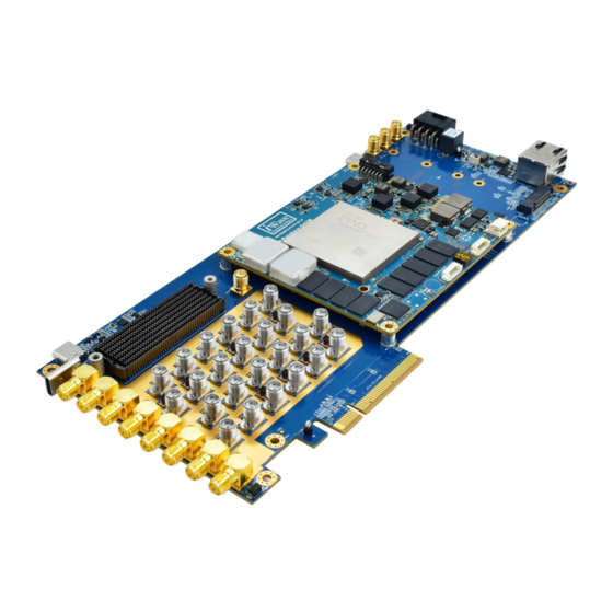
Summary of Contents for iWave iW-RainboW-G42P
- Page 1 Zynq-Ultrascale+ RFSoC (ZU29/39/49DR) SOM Development Platform Hardware User Guide iW-RainboW-G42P Zynq Ultrascale+ RFSoC (ZU29/39/49DR) SOM Development Platform Hardware User Guide REL0.3 iWave Systems Technologies Pvt. Ltd. Page 1 of 61...
- Page 2 (or authorized to receive for the recipient), you are hereby notified that any disclosure, copying distribution or use of any of the information contained within this document is STRICTLY PROHIBITED. Thank you. “iWave Systems Tech. Pvt. Ltd.”...
- Page 3 No warranty of accuracy is given concerning the contents of the information contained in this publication. To the extent permitted by law no liability (including liability to any person by reason of negligence) will be accepted by iWave Systems, its subsidiaries or employees for any direct or indirect loss or damage caused by omissions from or inaccuracies in this document.
-
Page 4: Table Of Contents
Mechanical Characteristics ........................57 3.4.1 Carrier Board Mechanical Dimensions ....................57 3.4.2 FAN Sink Fixing procedure on SOM with Carrier Board ................58 ORDERING INFORMATION ..........................59 APPENDIX ................................60 REL0.3 iWave Systems Technologies Pvt. Ltd. Page 4 of 61... - Page 5 Figure 19: Carrier board Mechanical dimension – Top and bottom view....................57 Figure 20: Board Mechanical dimension – Side View ..........................57 Figure 21: Zynq Ultrascale+ SOM with Fan sink fixing procedure ......................58 REL0.3 iWave Systems Technologies Pvt. Ltd. Page 5 of 61...
- Page 6 Table 10: Power Output Specification ..............................55 Table 11: Environmental Specification..............................56 Table 12: Orderable Product Part Numbers ............................59 Table 13: Low Pass Filters..................................60 Table 14: Band Pass Filters ..................................60 REL0.3 iWave Systems Technologies Pvt. Ltd. Page 6 of 61...
-
Page 7: Introduction
“iW-RainboW-G42M-Zynq-Ultrascale+RFSoC(ZU29,39,49DR)-SOM-HardwareUserGuide”. Overview iWave's Zynq Ultrascale+ RFSoC (ZU29/39/49DR) Development platform comes with Zynq Ultrascale+ RFSoC (ZU29/39/49DR) SOM and the RF-PCIe Carrier Board. The development board can be used for quick prototyping of RF and various applications targeted by the Zynq Ultrascale+ RFSoC (ZU29/39/49DR). - Page 8 Real Time Clock Right Receiver SDIO Secure Digital Input Output SDHI SD Card Host Interface System On Module Straight TXVR Transceiver Transmitter Universal Serial Bus USB OTG USB On The Go REL0.3 iWave Systems Technologies Pvt. Ltd. Page 8 of 61...
-
Page 9: References
Note: Signal Type does not include internal pull-ups or pull-downs implemented by the chip vendors and only includes the pull-ups or pull-downs implemented on board. References • Zynq Ultrascale+ RFSoC Datasheet & Reference Manual • Zynq Ultrascale+ RFSoC (ZU29/39/49DR) SOM Hardware User Guide REL0.3 iWave Systems Technologies Pvt. Ltd. Page 9 of 61... -
Page 10: Architecture And Design
Board To Board Connector1 USB 2.0 OTG (Optionally Connected) RTC Cell Header GTY x 8 PCIe Gen4 iWave Systems Technologies Pvt. Ltd. mktg@iwavesystems.com Figure 1: Zynq Ultrascale+ RFSoC (ZU29/39/49DR) SOM Carrier Board Block Diagram REL0.3 iWave Systems Technologies Pvt. Ltd. -
Page 11: Zynq Ultrascale+ Rfsoc (Zu29/39/49Dr) Som Carrier Board Features
➢ 4 Clock DIFF Capable LVDS/SE pins from HP Bank1 ➢ 10MHz REFCLK OUT x1 ➢ 1PPS_OUT x1 ➢ 4 VCM inputs for ADC Banks ➢ 1 DIFF Reference clock input for ADC & DAC. REL0.3 iWave Systems Technologies Pvt. Ltd. Page 11 of 61... - Page 12 General Specification • Power Supply ➢ 12V Through PCIex8 Edge Connector ➢ 12V Through 8 Pin ATX Power Connector • Form Factor : 254mm X 111.15mm (3/4 Length PCIe Card) REL0.3 iWave Systems Technologies Pvt. Ltd. Page 12 of 61...
-
Page 13: Board To Board Connectors
Board to Board Connector1 (J7) is physically located at the top of the board as shown below. Note: For the Board to Board Connector1 pinout, refer the Zynq Ultrascale+ RFSoC (ZU29/39/49DR) SOM Hardware User Guide. Figure 2: Board to Board Connector1 REL0.3 iWave Systems Technologies Pvt. Ltd. Page 13 of 61... -
Page 14: Board To Board Connector2
Board to Board Connector2 (J44) is physically located at the top of the board as shown below. Note: For the Board to Board Connector2 pinout, refer the Zynq Ultrascale+ RFSoC (ZU29/39/49DR) SOM Hardware User Guide. Figure 3: Board to Board Connector2 REL0.3 iWave Systems Technologies Pvt. Ltd. Page 14 of 61... -
Page 15: Ps Interface Features
Clock Generator” DSC557-0344FL1T”. This PCIe x4 M.2 Connector (J45) is physically located at the top of the board as shown below. Figure 4: PCIe x4 Connector REL0.3 iWave Systems Technologies Pvt. Ltd. Page 15 of 61... -
Page 16: Table 3: Pcie X4 M.2 Connector Pin Assignment
N/A5 PCIe Lane 2 Transmitter pair positive. This signal connected through PETp2 PCIe1_PETp2 O, DIFF MUX/DEMUX Chip. By default, Display port is configured through selection Pin. N/A6 Power Ground. N/A7 REL0.3 iWave Systems Technologies Pvt. Ltd. Page 16 of 61... - Page 17 O, DIFF (100 MHz) PEWAKE# BANK3_IO23N O, 3.3V CMOS This in is connected to PL IOs PCIe Reference Clock signals REFCLKP M2_PCIe1_REFCLKP O, DIFF (100 MHz) MFG1 Power Ground. MFG2 REL0.3 iWave Systems Technologies Pvt. Ltd. Page 17 of 61...
-
Page 18: Figure 5: Display Port Connector
The Display port connector supports AUX+ & AUX- signals from the PL Bank IOs. This Display Port connector (J5) is physically located at the top of the board as shown below. Figure 5: Display Port Connector REL0.3 iWave Systems Technologies Pvt. Ltd. Page 18 of 61... -
Page 19: Table 4: Display Port Type-C Pin Assignment
Display Port Transmit Lane1 Negative VBUS VBUS_DP Power 3.3V Power Supply. SBU2 BANK2_IO1N IO, 1.8V LVDS/ Auxiliary channel Negative. 100K, PU VBUS VBUS_DP Power 3.3V Power Supply. SSRXn1 SSRXp1 Power Ground REL0.3 iWave Systems Technologies Pvt. Ltd. Page 19 of 61... -
Page 20: Gigabit Ethernet Port1
(orange) and Link (Green) LED indications on RJ45 Magjack connector. This RJ45 Magjack connector(J36) is physically located at the top of the board as shown below. Figure 6: Gigabit Ethernet Connector1 REL0.3 iWave Systems Technologies Pvt. Ltd. Page 20 of 61... -
Page 21: Usb2.0 Otg Type-C Connector
B2B-2) and controls the power using the USB_PWR_EN pin (B32 pin of B2B-2). This USB2.0 OTG connector (J4) is physically located at the top of the board as shown below. Figure 7: USB OTG Connector REL0.3 iWave Systems Technologies Pvt. Ltd. Page 21 of 61... -
Page 22: Micro Sd Port
SD1_PWR/Bank6 IO16N is set to high, then 1.8V IO level is selected for SD1 signals to SD connector. The Standard SD connector (J48) is physically located at the bottom of the board as shown below. Figure 8: Standard SD Connector REL0.3 iWave Systems Technologies Pvt. Ltd. Page 22 of 61... -
Page 23: Usb Type-C Debug Connector (Jtag/Uart Usb Module)
‘BANK3_IO2P/ BANK3_IO2N’ are connected to UART PORT-3 of JTAG-SMT4. The USB TYPE-C Debug Connector(J6) can be used for Debug purpose which is is physically located at the top of the board as shown below. Figure 9: Debug UART Connector REL0.3 iWave Systems Technologies Pvt. Ltd. Page 23 of 61... -
Page 24: Interface Features
SMA connector are coming in the front panel 8 channel ( ADC0-CH0 to CH3, DAC0-CH0 to CH3). The 32 RF SMA Connector are located on the top of the PCB as shown below. Figure 10 : RF SMA Connectors REL0.3 iWave Systems Technologies Pvt. Ltd. Page 24 of 61... -
Page 25: Figure 11 : Rf Sampling Block Diagram
Transformer. The B2B Connector-1 to RF SMA connector pinout and BALUN informations are shown in the below mentioned Table 5 . Figure 11 : RF Sampling Block diagram Note: Please refer the Zynq Ultrascale+ RFSoC (ZU29/39/49DR) SOM user manual for more information REL0.3 iWave Systems Technologies Pvt. Ltd. Page 25 of 61... -
Page 26: Table 5 : Rf Sma Connectors Pinout
10MHz ~ 3GHz I, RF/SE-50E ADC3 – CH3 RF Input TCM2-33WX+ ADC3_CH3_N/Bank4 IO16N DAC0 Ports DAC0_CH0_N/Bank5 IO5N BD0810N50100AHF 800MHz ~ 1GHz DAC0 – CH0 RF Output O, RF/SE - DAC0_CH0_P/Bank5 IO5P REL0.3 iWave Systems Technologies Pvt. Ltd. Page 26 of 61... - Page 27 10MHz ~ 3GHz O, RF/SE - DAC3 – CH2 RF Output TCM2-33WX+ DAC3_CH2_N/Bank4 IO3N DAC3_CH3_P/Bank4 IO4P 10MHz ~ 3GHz O, RF/SE - DAC2 – CH3 RF Output TCM2-33WX+ DAC3_CH3_N/Bank4 IO4N REL0.3 iWave Systems Technologies Pvt. Ltd. Page 27 of 61...
-
Page 28: Fmc+ Hspc Connector
➢ 1 DIFF Reference clock input for DAC This 560Pin FMC+ HSPC connector (J11) is physically located at the top of the board as shown below. Figure 12: FMC+ HSPC Connector REL0.3 iWave Systems Technologies Pvt. Ltd. Page 28 of 61... -
Page 29: Figure 13: Fmc+ Hspc Connector Pin Out
* By default, FMC+ connector power is disabled as per Vita Specification. While booting the FMC or FMC+ Modules EEPROM is read and enabling the FMC+ connector power. * If FMC & FMC+ modules EEPROM is not programmed, then FMC+ connector power is not enabled. REL0.3 iWave Systems Technologies Pvt. Ltd. Page 29 of 61... -
Page 30: Table 6: Fmc+ Hpc Connector Pin Assignment
Board to Board Connector 2 A50 HS_TXVR0_TX1P O, DIFF differential transmitter positive. GTY Bank130 channel1 High speed DP1_C2M_N Board to Board Connector 2 A51 HS_TXVR0_TX1N O, DIFF differential transmitter negative. Ground. Power Ground. Power REL0.3 iWave Systems Technologies Pvt. Ltd. Page 30 of 61... - Page 31 This Pin is connected to PL Bank87 IO2 CLK_DIR Board to Board Connector 2 C44 BANK3_IO4P LVCMOS 3.3V positive Power Ground. Ground. Power DP9_M2C_P DP9_M2C_N Ground. Power Ground. Power DP8_M2C_P DP8_M2C_N Ground. Power Ground. Power REL0.3 iWave Systems Technologies Pvt. Ltd. Page 31 of 61...
- Page 32 Board to Board Connector 2 C53 HS_TXVR1_TX2P O, DIFF differential transmitter positive. GTY Bank131 channel2 High speed DP6_C2M_N Board to Board Connector 2 C54 HS_TXVR1_TX2N O, DIFF differential transmitter negative. REL0.3 iWave Systems Technologies Pvt. Ltd. Page 32 of 61...
- Page 33 PL Bank68 IO22 differential positive. LA27_P Board to Board Connector 2 D20 BANK1_IO3P IO, 1.8V PL Bank93 IO22 differential negative . LA27_N Board to Board Connector 2 D21 BANK1_IO3N Ground. Power Ground. Power REL0.3 iWave Systems Technologies Pvt. Ltd. Page 33 of 61...
- Page 34 IO, 1.8V PL Bank67 IO14 differential positive. LA17_P_CC Board to Board Connector 1 D11 BANK0_IO14P/GCIN3P IO, 1.8V PL Bank67 IO14 differential negative . LA17_N_CC Board to Board Connector 1 D12 BANK0_IO14N/GCIN3N REL0.3 iWave Systems Technologies Pvt. Ltd. Page 34 of 61...
- Page 35 PL Bank68 IO13 differential positive. HA01_P_CC Board to Board connector 1 BANK1_IO13P/GCIN1P IO, 1.8V HA01_N_CC Board to Board connector 1 BANK1_IO13N/GCIN1N IO, 1.8V PL Bank68 IO13 differential negative Ground. Power REL0.3 iWave Systems Technologies Pvt. Ltd. Page 35 of 61...
- Page 36 Carrier Board Supply Voltage. VADJ VCC_FMC+_ADJ O, 1.8V Power Power Ground. Power Good Signal from FMC Module to I, 3.3V CMOS/ PG_M2C Board to Board Connector 1 B55 BANK3_IO21P AP12 10K PU Carrier. REL0.3 iWave Systems Technologies Pvt. Ltd. Page 36 of 61...
- Page 37 Power HB04_P HB04_N Ground. Power HB08_P HB08_N Ground. Power HB12_P HB12_N Ground. Power HB16_P HB16_N Ground. Power HB20_P HB20_N Ground. Power Carrier Board Supply Voltage. VADJ VCC_FMC+_ADJ O, 1.8V Power REL0.3 iWave Systems Technologies Pvt. Ltd. Page 37 of 61...
- Page 38 Board to Board Connector 1 B18 BANK1_IO8P IO, 1.8V PL Bank68 IO20 differential negative. LA33_N Board to Board Connector 1 B19 BANK1_IO8N Ground. Power Carrier Board Supply Voltage. VADJ VCC_FMC+_ADJ O, 1.8V Power REL0.3 iWave Systems Technologies Pvt. Ltd. Page 38 of 61...
- Page 39 PL Bank67 IO1 differential negative. LA30_N Board to Board Connector 1 A14 BANK0_IO24N Ground. Power IO, 1.8V PL Bank68 IO19 differential positive. LA32_P Board to Board Connector 1 B16 BANK1_IO7P REL0.3 iWave Systems Technologies Pvt. Ltd. Page 39 of 61...
- Page 40 Board to Board Connector 1 D26 BANK1_IO14N/GCIN3N Ground. Power HA22_P HA22_N Ground. Power HB01_P HB01_N Ground. Power HB07_P HB07_N Ground. Power HB11_P HB11_N Ground. Power HB15_P HB15_N Ground. Power HB18_P REL0.3 iWave Systems Technologies Pvt. Ltd. Page 40 of 61...
- Page 41 Board to Board Connector 1 A21 BANK1_IO12N_GCIN0N IO, 1.8V Ground. Power HA21_P HA21_N Ground. Power HA23_P HA23_N Ground. Power HB00_P_CC HB00_N_CC Power Ground. HB06_P_CC HB06_N_CC Ground. Power HB10_P HB10_N Ground. Power HB14_P HB14_N REL0.3 iWave Systems Technologies Pvt. Ltd. Page 41 of 61...
- Page 42 10 MHz clock output from SOM clock REFCLK_C2M_P Board to Board Connector 2 D11 MSIO3/10MHz_REFCLK_OUT O, 3.3V synthesiser(ZL30733LDG1). REFCLK_C2M_N Power Ground. Ground. Power REFCLK_M2C_P REFCLK_M2C_N Ground. Power Ground. Power SYNC_M2C_P SYNC_M2C_N Ground. Power Ground. Power RES2 REL0.3 iWave Systems Technologies Pvt. Ltd. Page 42 of 61...
- Page 43 Power Ground. Ground. Power DP20_M2C_P DP20_M2C_N Ground. Power Ground. Power DP14_C2M_P DP14_C2M_N Ground. Power Power Ground. DP15_C2M_P DP15_C2M_N Ground. Power Ground. Power DP16_C2M_P DP16_C2M_N Power Ground. Ground. Power DP17_C2M_P DP17_C2M_N REL0.3 iWave Systems Technologies Pvt. Ltd. Page 43 of 61...
- Page 44 Power Ground. Power Ground. DP14_M2C_P Power DP14_M2C_N Power Ground. Ground. Power Ground. Power Ground. DP15_M2C_P Power Ground. DP15_M2C_N Power Ground. Power Ground. Power DP11_C2M_P DP11_C2M_N Ground. Power Ground. Power DP13_C2M_P REL0.3 iWave Systems Technologies Pvt. Ltd. Page 44 of 61...
- Page 45 Power Ground. Ground. Power DP11_M2C_P DP11_M2C_N Ground. Power Ground. Power DP13_M2C_P DP13_M2C_N Ground. Power Ground. Power GBTCLK5_M2C_P GBTCLK5_M2C_N Ground. Power Ground. Power DP10_C2M_P DP10_C2M_N Power Ground. Ground. Power DP12_C2M_P DP12_C2M_N REL0.3 iWave Systems Technologies Pvt. Ltd. Page 45 of 61...
- Page 46 Note: * FMC+ connector supports VADJ 1.8V and 1.2V. By default, VADJ is set to 1.8V. Contact iWave for further details. * If VCC_FMC+_ADJ voltage changed from default value 1.8 to 1.2V, Please make sure that SOM concern IO voltage also to be modified to avoid IO conflict.
-
Page 47: Pcie X8 Edge Connector
JTAG_TDI JTAG_TDO JTAG_TMS +3_3V 3.3V Power 3.3V PCIe Supply. +3_3V 3.3V Power 3.3V PCIe Supply. PERST_N IO_T3U_N12_65 AL20 I, 3.3V, PCIe Reset Signal. This pin is connected through level translator REL0.3 iWave Systems Technologies Pvt. Ltd. Page 47 of 61... - Page 48 PCIe Transmitter Differential Pair Lane4 Positive. PER4N MGTYTXN0_129 O, DIFF PCIe Transmitter Differential Pair Lane4 Negative. Power Ground. Power Ground. PER5P MGTYTXP1_129 O, DIFF PCIe Transmitter Differential Pair Lane5 Positive. REL0.3 iWave Systems Technologies Pvt. Ltd. Page 48 of 61...
- Page 49 Ground. PRSNT2n_X1 Power Ground. PET1P MGTYRXP1_128 AB39 I, DIFF PCIe Receiver Differential Pair Lane1 Positive. PET1N MGTYRXN1_128 AB40 I, DIFF PCIe Receiver Differential Pair Lane1 Negative. Power Ground. Power Ground. REL0.3 iWave Systems Technologies Pvt. Ltd. Page 49 of 61...
- Page 50 Pair Lane7 Positive. PET7N MGTYRXN3_129 I, DIFF PCIe Transmitter Differential Pair Lane7 Negative. Power Ground. PRSNT2n_X8 IO, CMOS PCIe Hot Plug Detect. Connected to A1st pin of J47. Power Ground. REL0.3 iWave Systems Technologies Pvt. Ltd. Page 50 of 61...
-
Page 51: Additional Features
System Sync Clock Input pin of B2B connector-2, the J1 SMA Connector is connected to 1PPS inpt pin of B2B connector-2. The pinout details for this SMA connector are metioned in the below table. Figure 15 : Sync and Reference Clock SMA connectors REL0.3 iWave Systems Technologies Pvt. Ltd. Page 51 of 61... -
Page 52: Reset Push Button
(ZU29/39/49DR) CPU. Reset signal of Board to Board connector2 Pin B14 is directly connected from Reset Push button switch. This Reset Push button switch (SW3) is physically located at the top of the board as shown below. Figure 16 : Reset Push Button REL0.3 iWave Systems Technologies Pvt. Ltd. Page 52 of 61... -
Page 53: Rtc Cell Header
Ultrascale+ RFSoC (ZU29/39/49DR) SOM for RTC back up voltage when VCC main power is off. This Coin Cell Holder (J20) is physically located at the top of the board as shown below. Figure 17: RTC Coin Cell Holder REL0.3 iWave Systems Technologies Pvt. Ltd. Page 53 of 61... -
Page 54: Technical Specification
VCC_12V_TRP2 11.75V 12.25V ±50mV VRTC_3V0¹ 3.15V ±20mV ¹ The Zynq Ultrascale+ RFSoC (ZU29/39/49DR) DevKit uses this voltage as backup power source to On-SOM PMIC RTC controller when VCC is off. REL0.3 iWave Systems Technologies Pvt. Ltd. Page 54 of 61... -
Page 55: Power Output Specification
Carrier Board. For SOM Power consumption, please refer our SOM Hardware user Guide. VRTC_3V0 3.15V To FMC+ Connector VCC_FMC_ADJ 1.75 1.85 VCC_3V3 3.15 3.45 3P3VAUX 3.15 3.45 100mA VCC_12V 11.75V 12.25V REL0.3 iWave Systems Technologies Pvt. Ltd. Page 55 of 61... -
Page 56: Environmental Characteristics
3.3.3 Electrostatic Discharge iWave’s Zynq Ultrascale+ RFSoC (ZU29/39/49DR) Development platform is sensitive to electro static discharge and so high voltages caused by static electricity could damage some of the devices on board. It is packed with necessary protection while shipping. Do not open or use board except at an electrostatic free workstation. -
Page 57: Mechanical Characteristics
Ethernet Connector (15.28mm) and bottom side maximum height component height is (2.5mm). Please refer the below figure for height details of the Zynq Ultrasclae+ RFSoC (ZU29/39/49DR) Carrier. Figure 20: Board Mechanical dimension – Side View REL0.3 iWave Systems Technologies Pvt. Ltd. Page 57 of 61... -
Page 58: Fan Sink Fixing Procedure On Som With Carrier Board
3.4.2 FAN Sink Fixing procedure on SOM with Carrier Board The RF PCIe Carrier Card and Zynq Ultrascale+ RFSoC SOM with Fan sink fixing procedure is shown below. Figure 21: Zynq Ultrascale+ SOM with Fan sink fixing procedure REL0.3 iWave Systems Technologies Pvt. Ltd. Page 58 of 61... -
Page 59: Ordering Information
ZU29DR -1 RFSoC with 8GB PS DDR4, 8GB FPGA DDR4, 32GB eMMC Industrial SOM – PCIe Dev.kit with Linux Note: For Development platform identification purpose, Product part number is pasted as Label with Barcode readable format. REL0.3 iWave Systems Technologies Pvt. Ltd. Page 59 of 61... -
Page 60: Appendix
Table 14: Band Pass Filters Parameters Value Part Numbers VBFZ-3590-S+ Manufacturer Mini-Circuits Description Signal Conditioning BANDPASS FLTR / SMA / RoHS Impedance 50 OHM Frequency Range 3000 MHz to 4300 MHz Quantity REL0.3 iWave Systems Technologies Pvt. Ltd. Page 60 of 61... - Page 61 Zynq-Ultrascale+ RFSoC (ZU29/39/49DR) SOM Development Platform Hardware User Guide REL0.3 iWave Systems Technologies Pvt. Ltd. Page 61 of 61...
Need help?
Do you have a question about the iW-RainboW-G42P and is the answer not in the manual?
Questions and answers