iWave Zynq Ultrascale+ iW-RainboW-G36S Hardware User's Manual
Mpsoc sbc hardware
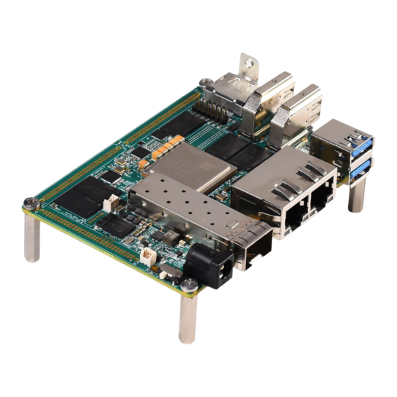
Hide thumbs
Also See for Zynq Ultrascale+ iW-RainboW-G36S:
- Quick start manual (19 pages) ,
- Quick start manual (21 pages) ,
- Hardware user's manual (88 pages)

Related Manuals for iWave Zynq Ultrascale+ iW-RainboW-G36S


Summary of Contents for iWave Zynq Ultrascale+ iW-RainboW-G36S
- Page 1 Zynq Ultrascale+ MPSoC SBC Hardware User Guide iW-RainboW-G36S Zynq Ultrascale+ MPSoC SBC Hardware User Guide REL0.2 iWave Systems Technologies Pvt. Ltd. Page 1 of 88...
- Page 2 If you are not the intended recipient (or authorized to receive for the recipient), you are hereby notified that any disclosure, copying distribution or use of any of the information contained within this document is STRICTLY PROHIBITED. Thank you. “iWave Systems Tech. Pvt. Ltd.” REL0.2 iWave Systems Technologies Pvt.
- Page 3 No warranty of accuracy is given concerning the contents of the information contained in this publication. To the extent permitted by law no liability (including liability to any person by reason of negligence) will be accepted by iWave Systems, its subsidiaries or employees for any direct or indirect loss or damage caused by omissions from or inaccuracies in this document.
-
Page 4: Table Of Contents
2.8.4 3G/12G SDI IN (Optional) ..........................37 2.8.5 3G/12G SDI Output (Optional) ........................37 Additional Features ............................38 2.9.1 Clock Synthesizers ............................38 2.9.2 JTAG Header ..............................38 2.9.3 Fan Header ..............................40 REL0.2 iWave Systems Technologies Pvt. Ltd. Page 4 of 88... - Page 5 3.3.2 RoHS2 Compliance ............................82 3.3.3 Electrostatic Discharge ..........................82 3.3.4 Heat Sink ..............................82 MechanicalCharacteristics ..........................83 3.4.1 Zynq Ultrascale+ MPSoC SBC Mechanical Dimensions ................83 ORDERING INFORMATION .......................... 85 REL0.2 iWave Systems Technologies Pvt. Ltd. Page 5 of 88...
- Page 6 Figure 23: Mechanical dimension of Zynq Ultrascale+ MPSoC SBC - Top View.............. 83 Figure 24: Mechanical dimension of Zynq Ultrascale+ MPSoC SBC - Bottom View ............83 Figure 25: Mechanical dimension of Zynq Ultrascale+ MPSoC SBC - Side View ............. 84 REL0.2 iWave Systems Technologies Pvt. Ltd. Page 6 of 88...
- Page 7 Table 15: Power Input Requirement ..........................80 Table 16: Power Output Specification ..........................81 Table 17: Power Consumption¹ ............................81 Table 18: Temperature Specification ..........................82 Table 19: Orderable Product Part Numbers ........................85 REL0.2 iWave Systems Technologies Pvt. Ltd. Page 7 of 88...
-
Page 8: Introduction
This document is the Hardware User Guide for the Zynq Ultrascale+ MPSoC Single Board Computer based on the Xilinx Zynq Ultrascale+ MPSoC . This board is fully supported by iWave Systems Technologies Pvt. Ltd. This Guide provides detailed information on the overall design and usage of the Zynq Ultrascale+ MPSoC SBC from a Hardware Systems perspective. - Page 9 Secure Digital Input Output System On Chip Serial Peripheral Interface UART Universal Asynchronous Receiver/Transmitter ULPI UTMI+ Low Pin Interface Universal Serial Bus USB OTG USB On The Go UTMI USB2.0 Transceiver Macrocell Interface REL0.2 iWave Systems Technologies Pvt. Ltd. Page 9 of 88...
-
Page 10: Terminlogy Description
Note: Signal Type does not include internal pull-ups or pull-downs implemented by the chip vendors and only includes the pull-ups or pull-downs implemented On-SBC. References • Zynq Ultrascale+ MPSoC Technical Reference Manual • Zynq Ultrascale+ MPSoC Device Overview REL0.2 iWave Systems Technologies Pvt. Ltd. Page 10 of 88... -
Page 11: Architecture And Design
GTH Transceiver block is supported in ZU4 & ZU5 MPSoC with data rates up to 12.5Gb/s. GTH transceiver block is not supported in ZU2 & ZU3 MPSoC. “ “ This symbol indicates Hardware assembly options available in the board and by default which option is support ed. Contact iWave to support other assembly option. Figure 1: Zynq Ultrascale+ MPSoC SBC Block Diagram REL0.2... -
Page 12: Zynq Ultrascale+ Mpsoc Sbc Features
EEPROM For MAC Address • Micro SD Connector (Optional) Features from PS Block • Dual 10/100/1000Mbps Ethernet through RJ45 Magjack • WLAN & BT Module with Antenna connector • Debug UART Header REL0.2 iWave Systems Technologies Pvt. Ltd. Page 12 of 88... - Page 13 Variable IO voltage support from 1.2V to 1.8V • PL IOs - HD Bank45 ⁵ ➢ Upto 4 Single ended (SE) IOs o Variable IO voltage support from 1.2V to 3.3V REL0.2 iWave Systems Technologies Pvt. Ltd. Page 13 of 88...
- Page 14 ➢ Upto 12 LVDS IOs/24 Single ended (SE) IOs o Upto 4 GC Global Clock Input pins (LVDS/SE) o Upto 8 ADC Input pins (Differential/Single Ended) o Variable IO voltage support from 1.2V to 3.3V REL0.2 iWave Systems Technologies Pvt. Ltd. Page 14 of 88...
- Page 15 In Zynq Ultrascale+ MPSoC SBC, GTH Transceiver Channel3 is shared with SFP+ and SDI In & Out. So either SFP+ or SDI IN & Out only can be supported. By default SFP+ is supported in SBC. Contact iWave to support SDI IN & Out.
-
Page 16: Zynq Ultrascale+ Mpsoc
Figure 2: Zynq Ultrascale+ MPSoC CPU Simplified Block Diagram Note: Please refer the latest Zynq Ultrascale+ MPSoC Datasheet & Technical Reference Manual for more details which may be revised from time to time. REL0.2 iWave Systems Technologies Pvt. Ltd. Page 16 of 88... -
Page 17: Figure 3: Zynq Ultrascale+ Mpsoc Devices Comparison
MPSoC to route most of the IO peripheral interfaces to PL Bank I/O pins referred as EMIO (Extended MIO). Zynq Ultrascale+ MPSoC’s PS Peripheral Pin mapping options between MIO & EMIO is shown below. REL0.2 iWave Systems Technologies Pvt. Ltd. Page 17 of 88... -
Page 18: Mpsoc Power
Board Connectors are generated from PMIC LDO1 and LDO6, LDO3, LDO4, & LDO7 respectively. By default, HP Banks and HD Banks voltages are set to 1.2V and configurable through software after bootup REL0.2 iWave Systems Technologies Pvt. Ltd. Page 18 of 88... -
Page 19: Mpsoc Reset
I/O voltage of PL Bank43 is set between 1.8V to 3.3V. ² Mentioned voltage level is based on after uboot bootup I/O voltage set to PL Bank43. REL0.2 iWave Systems Technologies Pvt. Ltd. Page 19 of 88... -
Page 20: Mpsoc Configuration & Status
SD1, USB0 & JTAG as boot device and configurable through mode pins. Upon device reset, MPSoC mode pins are read to determine the primary boot device. By default, eMMC is supported as boot device in SBC. REL0.2 iWave Systems Technologies Pvt. Ltd. Page 20 of 88... -
Page 21: Mpsoc System Monitor/Adc
The PMIC supports Real Time Clock functionality through J6 connector for RTC backup power. The PMIC can support backup battery charging to charge Lithium-Manganese coin cell batteries and super capacitors if required. REL0.2 iWave Systems Technologies Pvt. Ltd. Page 21 of 88... -
Page 22: Memory
The Zynq Ultrascale+ MPSoC SBC supports 256kb EEPROM for MAC Address. The I2C0 module of Zynq Ultrascale+ MPSoC PS is used for EEPROM interface through MIO pins with I2C address 0x50. This device operates at 1.8 voltage level. REL0.2 iWave Systems Technologies Pvt. Ltd. Page 22 of 88... -
Page 23: Micro Sd Connector (Optional)
Zynq Ultrascale+ MPSoC PS. If PS_MIO43_501 is set to low, then 3.3V IO level is selected for SD1 signals to SD connector. If PS_MIO43_501 is set to high, then 1.8V IO level is selected for SD1 signals to SD connector. REL0.2 iWave Systems Technologies Pvt. Ltd. Page 23 of 88... -
Page 24: Fearures From Ps Block
Magjack port. This Dual port RJ45 Magjack (J15) is physically located at the top of the board as shown below. Figure 5: Dual Gigabit Ethernet Port * Same MDC and MDIO control signals are shared to GEM0 & GEM3 external Gigabit Ethernet PHY. REL0.2 iWave Systems Technologies Pvt. Ltd. Page 24 of 88... -
Page 25: Wlan & Bt Module With Antenna Connector
Note: In Zynq Ultrascale+ MPSoC SBC, SD1 signals from MPSoC is shared with WLAN module and MicroSD connector. So either WLAN or Micro SD connector can be supported. By default WLAN module is supported in SBC. Contact iWave to support Micro SD connector. -
Page 26: Debug Uart Header
Bank Termination UART0_TX PS_MIO07 AH17 O, 3.3V LVCMOS UART0 Transmit data line _500 for Debug. UART0_RX PS_MIO06 AF16 I, 3.3V LVCMOS UART0 Receive data line _500 for Debug. Power Ground. REL0.2 iWave Systems Technologies Pvt. Ltd. Page 26 of 88... -
Page 27: Features From Ps-Gtr
The Display port connector supports AUX+ & AUX- signals from the PL Bank IOs. Also it supports Hot plug detect signal and connected to PL Bank IO. This Display Port connector (J5) is physically located at the top of the board as shown below. Figure 8: Display Port Connector REL0.2 iWave Systems Technologies Pvt. Ltd. Page 27 of 88... -
Page 28: Dual Usb3.0 Type A Jack
On/Off the power based on the Host and also limits the current above 900mA in host mode. This dual stack USB Type-A connector (J17) is physically located at the top of the board as shown below. Figure 9: Dual Stack USB3.0 Type-A Jack REL0.2 iWave Systems Technologies Pvt. Ltd. Page 28 of 88... -
Page 29: Key B Connector With Sata & Usb3.0
HUB. MPSoC’s SATA supports SATA Specification revision 3.1 with Gen1(1.5Gbps), Gen2(3Gbps) & Gen3(6Gbps) datarates. This M.2 connector (J27) is physically located at the bottom of the board as shown below. Figure 10: M.2 Key B Connector REL0.2 iWave Systems Technologies Pvt. Ltd. Page 29 of 88... -
Page 30: Table 5: M.2 Connector Pin Assignment
Power Ground GPIO5 CONFIG_0 M.2 Configuration Pin 0. GPIO6 GPIO11 GPIO7 1.8V M.2 Dynamic Power Reduction CMOS Signal. This signal is configuring from PMIC GPIO1 (U14). GPIO10 Power Ground. GPIO8 REL0.2 iWave Systems Technologies Pvt. Ltd. Page 30 of 88... - Page 31 3_505 GPIO2 Power Ground. GPIO3 PETN0/SATA_A PS_MGTRTXN O, DIFF SATA Transmit pair negative. 3_505 GPIO4 PETP0/SATA_A PS_MGTRTXP3 O, DIFF SATA Transmit pair Positive. _505 PERST# Power Ground. CLKREQ# REFCLKN PEWAKE# REL0.2 iWave Systems Technologies Pvt. Ltd. Page 31 of 88...
- Page 32 Oscillator is connected to this pin CONFIG_1 M.2 Configuration Pin 1. VCC_3V3 3.3V Supply Voltage. Power Power Ground. VCC_3V3 3.3V Supply Voltage. Power Power Ground. VCC_3V3 3.3V Supply Voltage. Power CONFIG_2 M.2 Configuration Pin 2. REL0.2 iWave Systems Technologies Pvt. Ltd. Page 32 of 88...
-
Page 33: Features From Pl-Gth
Important Note: In Zynq Ultrascale+ MPSoC SBC, GTH Transceiver Channel3 is shared with SFP+ and SDI In & Out. So either SFP+ or SDI IN & Out only can be supported. By default SFP+ is supported in SBC. Contact iWave to support SDI IN &... -
Page 34: Hdmi Output Connector
(SN65DP159RGZR) and then connected to HDMI Out Connector for HDMI out. This HDMI Out connector can support upto 4K@60 resolution. This HDMI Out connector (J11) is physically located at the top of the board as shown below. Figure 12: HDMI Out Connector REL0.2 iWave Systems Technologies Pvt. Ltd. Page 34 of 88... -
Page 35: Sfp+ Connector
Important Note: In Zynq Ultrascale+ MPSoC SBC, GTH Transceiver Channel3 is shared with SFP+ and SDI In & Out. So either SFP+ or SDI IN & Out only can be supported. By default SFP+ is supported in SBC. Contact iWave to support SDI IN &... -
Page 36: Table 6: Sfp+ Connector Pin Assignment
3.3V Receiver Supply Voltage. Power VCCT 3.3V 3.3V Transmitter Supply Voltage. Power VEET2 Power Ground. MGTHTXP3_2 O, DIFF SFP+ Transmit Data Positive. MGTHTXN3_2 O, DIFF SFP+ Transmit Data Negative. VEET3 Power Ground. REL0.2 iWave Systems Technologies Pvt. Ltd. Page 36 of 88... -
Page 37: 12G Sdi In (Optional)
Important Note: In Zynq Ultrascale+ MPSoC SBC, GTH Transceiver Channel3 is shared with SFP+ and SDI In & Out. So either SFP+ or SDI IN & Out only can be supported. By default SFP+ is supported in SBC. Contact iWave to support SDI IN &... -
Page 38: Additional Features
Zynq Ultrascale MPSoC. These JTAG interface signals are at 3.3V Voltage level. The JTAG Header (J3) is physically located on topside of the SBC as shown below. JTAG-HS2 Programming Cable can be directly connected to this JTAG Header. REL0.2 iWave Systems Technologies Pvt. Ltd. Page 38 of 88... -
Page 39: Figure 14: Jtag Header
JTAG Test Clock. 49.9K PU Power Ground. JTAG_TDO O, 3.3V LVCMOS JTAG Test Data Output. Power Ground. JTAG_TDI I, 3.3V LVCMOS/ JTAG Test Data Input. 49.9K PU Power Ground. Power Ground. JTAG_RESETB REL0.2 iWave Systems Technologies Pvt. Ltd. Page 39 of 88... -
Page 40: Fan Header
Figure 15: Fan Header Table 9: Fan Header Pinout SoC Ball Name/ Signal Type/ Pin No Pin Name Description Pin Number Termination VCC_5V O, 5V Power Supply Voltage. Power Ground. REL0.2 iWave Systems Technologies Pvt. Ltd. Page 40 of 88... -
Page 41: Rtc Header
Figure 16: RTC Header Table 10: RTC Header Pinout SoC Ball Name/ Signal Type/ Pin No Pin Name Description Pin Number Termination VRTC_3V0 O, 3V Power Supply Voltage. Power Ground. REL0.2 iWave Systems Technologies Pvt. Ltd. Page 41 of 88... -
Page 42: Power On/Off Switch
Zynq Ultrascale+ MPSoC is directly connected from Reset Push button switch. This Reset Push button switch (SW2) is physically located at the top of the board as shown below. Figure 18: Reset Switch REL0.2 iWave Systems Technologies Pvt. Ltd. Page 42 of 88... -
Page 43: Board To Board Connector1
Connector1 (J21) is physically located on bottom side of the SBC as shown below. Number of Pins - 60 Connector Part Number - TFC-130-11-L-D-A Mating Connector - SFC-130-T1-L-D-A from Samtech Staking Height - 7.75mm Figure 19: Board to Board Connector1 REL0.2 iWave Systems Technologies Pvt. Ltd. Page 43 of 88... -
Page 44: Table 11: Board To Board Connector1 Pinout
SPI0_SS0(PS_MIO3_500) PL_AG5_LVDS64_L10N_QBC SPI0_SCLK(PS_MIO0_500) PL_AG6_LVDS64_L10P_QBC I2C1_SCL(PS_MIO24_500) I2C1_SDA(PS_MIO25_500) PL_AH7_LVDS64_L9N PL_AH8_LVDS64_L9P CAN1_RX(PS_MIO41_501) CAN0_TX(PS_MIO39_501) PL_AH9_LVDS64_L7N_QBC CAN1_TX(PS_MIO40_501) PL_AG9_LVDS64_L7P_QBC CAN0_RX(PS_MIO38_501) PL_AE8_LVDS64_L2N PL_AG8_LVDS64_L8N PL_AE9_LVDS64_L2P PL_AF8_LVDS64_L8P PL_AE7_LVDS64_L4N_DBC PL_AD9_LVDS64_L1N_DBC PL_AD7_LVDS64_L4P_DBC PL_AC9_LVDS64_L1P_DBC PL_AC8_LVDS64_L3N PL_AC7_LVDS64_L5N PL_AB8_LVDS64_L3P PL_AB7_LVDS64_L5P PL_AB6_LVDS64_L6P PL_AC6_LVDS64_L6N VCC_5V VCC_1V8 REL0.2 iWave Systems Technologies Pvt. Ltd. Page 44 of 88... -
Page 45: Ps Interfaces
CAN1_TX(PS_MIO4 PS_MIO40 O, 1.8V LVCMOS CAN1 Transmit data. 0_501) _501 CAN0_TX(PS_MIO3 PS_MIO39 O, 1.8V LVCMOS CAN0 Transmit data. 9_501) _501 CAN0_RX(PS_MIO3 PS_MIO38 I, 1.8V LVCMOS CAN0 Receive data. 8_501) _501 REL0.2 iWave Systems Technologies Pvt. Ltd. Page 45 of 88... -
Page 46: I2C Interface
Connector1 pins 1, 3, 7, 9, 13, and 15 are HDGC Global Clock Input capable pins of PL Bank64. Also Board to Board Connector1 pins 19, 21, 25, 27, 31, 33, 43, 45, 49, 51, 55, 57, 38, 40, 50, and 52 are PLSYSMON auxiliary analog Input capable pins of PL Bank64. REL0.2 iWave Systems Technologies Pvt. Ltd. Page 46 of 88... - Page 47 Clock Input differential positive or Single ended I/O. PL_AD5_LVDS64_ IO_L13P_T2L_N0_G IO, 1.8V LVDS Bank64 IO13 L13P_GC C_QBC_64 differential positive. Same configured as HDGC Global Clock Input differential positive or Single ended I/O. REL0.2 iWave Systems Technologies Pvt. Ltd. Page 47 of 88...
- Page 48 Single ended I/O. PL_AH9_LVDS64_ IO_L7N_T1L_N1_Q IO, 1.8V LVDS PL Bank64 IO7 differential L7N_QBC BC_AD13N_64 negative. Same configured as PLSYSMON differential analog input13 Negative or Single ended I/O. REL0.2 iWave Systems Technologies Pvt. Ltd. Page 48 of 88...
- Page 49 Single ended I/O. PL_AC8_LVDS64_ IO_L3N_T0L_N5_A IO, 1.8V LVDS PL Bank64 IO3 differential D15N_64 negative. Same configured as PLSYSMON differential analog input15 Negative or Single ended I/O. REL0.2 iWave Systems Technologies Pvt. Ltd. Page 49 of 88...
- Page 50 Same configured as PLSYSMON differential analog input5 positive or Single ended I/O. PL_AD9_LVDS64_ IO_L1N_T0L_N1_D IO, 1.8V LVDS PL Bank64 IO1 differential L1N_DBC BC_64 negative. Same configured as Single ended I/O. REL0.2 iWave Systems Technologies Pvt. Ltd. Page 50 of 88...
-
Page 51: Ios - Hd Bank45
Note: In ZCU2 & ZCU3 MPSoC devices, the PL Bank 43, 44, 45 & 46 is called as 44, 24, 25 & 26 respectively. Only the Bank Numbering is different and all other functionalities remain same. REL0.2 iWave Systems Technologies Pvt. Ltd. Page 51 of 88... -
Page 52: Power
O, 5V Power 5V Supply Voltage. VCC_1V8 O, 1.8V 1.8V Supply Voltage. Power 5, 11, 17, 23, 29, 35, 41, 47, Power Ground. 53, 59, 26, 36, 42, 48, 54, REL0.2 iWave Systems Technologies Pvt. Ltd. Page 52 of 88... -
Page 53: Board To Board Connector2
Connector2 (J22) is physically located on bottom side of the SBC as shown below. Number of Pins - 60 Connector Part Number - TFC-130-11-L-D-A Mating Connector - SFC-130-T1-L-D-A from Samtech Staking Height - 7.75mm Figure 20: Board to Board Connector2 REL0.2 iWave Systems Technologies Pvt. Ltd. Page 53 of 88... -
Page 54: Table 12: Board To Board Connector2 Pinout
PL_B15_LVDS46_L1P PL_A15_LVDS46_L1N PL_D15_LVDS46_L5P_GC PL_D14_LVDS46_L5N_GC PL_C14_LVDS46_L4P PL_C13_LVDS46_L4N PL_B14_LVDS46_L2P PL_A14_LVDS46_L2N PL_B13_LVDS46_L3P PL_A13_LVDS46_L3N PL_E14_LVDS46_L6P_GC PL_E13_LVDS46_L6N_GC PL_F15_LVDS46_L8P_HDGC PL_E15_LVDS46_L8N_HDGC PL_G13_LVDS46_L7P_GC PL_F13_LVDS46_L7N_GC PL_H14_LVDS46_L10P PL_H13_LVDS46_L10N PL_H11_LVDS45_L3P PL_G10_LVDS45_L3N PL_J12_LVDS45_L4P PL_H12_LVDS45_L4N PL_J11_LVDS45_L1P PL_J10_LVDS45_L1N PL_K13_LVDS45_L2P PL_K12_LVDS45_L2N VCC_5V SYSMON_VP VCC_12V SYSMON_VN REL0.2 iWave Systems Technologies Pvt. Ltd. Page 54 of 88... -
Page 55: Interfaces
Same configured as PLSYSMON differential analog input9 negative or Single ended I/O. PL_AF1_LVDS64_ IO_L24P_T3U_N10 IO, 1.8V LVDS Bank64 IO24 L24P differential positive. Same configured as Single ended I/O. REL0.2 iWave Systems Technologies Pvt. Ltd. Page 55 of 88... - Page 56 Single ended I/O. PL_AB1_LVDS64_ IO_L18P_T2U_N10 IO, 1.8V LVDS Bank64 IO18 L18P _AD2P_64 differential positive. Same configured as PLSYSMON differential analog input2 positive or Single ended I/O. REL0.2 iWave Systems Technologies Pvt. Ltd. Page 56 of 88...
- Page 57 Clock Input differential positive or Single ended I/O. PL_AC3_LVDS64_ IO_L14N_T2L_N3_ IO, 1.8V LVDS Bank64 IO14 L14N_GC GC_64 differential negative. Same configured as HDGC Global Clock Input differential negative or Single ended I/O. REL0.2 iWave Systems Technologies Pvt. Ltd. Page 57 of 88...
-
Page 58: Ios -Hd Bank45
Single ended I/O. PL_G10_LVDS45_ IO_L3N_AD13N_45 IO, 1.8V LVDS PL Bank45 IO3 differential negative. Same configured as PLSYSMON differential analog input13 negative or Single ended I/O. REL0.2 iWave Systems Technologies Pvt. Ltd. Page 58 of 88... - Page 59 Single ended I/O. PL_K12_LVDS45_ IO_L2N_AD14N_45 IO, 1.8V LVDS PL Bank45 IO2 differential negative. Same configured as PLSYSMON differential analog input14 negative or Single ended I/O. REL0.2 iWave Systems Technologies Pvt. Ltd. Page 59 of 88...
-
Page 60: Ios -Hd Bank46
PLSYSMON differential analog input1 positive or Single ended I/O. PL_J14_LVDS46_L IO_L11N_AD1N_46 IO, 1.8V LVDS Bank46 IO11 differential negative. Same configured as PLSYSMON differential analog input1 negative or Single ended I/O. REL0.2 iWave Systems Technologies Pvt. Ltd. Page 60 of 88... - Page 61 Single ended I/O. PL_A15_LVDS46_ IO_L1N_AD11N_46 IO, 1.8V LVDS PL Bank46 IO1 differential negative. Same configured as PLSYSMON differential analog input11 negative or Single ended I/O. REL0.2 iWave Systems Technologies Pvt. Ltd. Page 61 of 88...
- Page 62 Single ended I/O. PL_B14_LVDS46_ IO_L2P_AD10P_46 IO, 1.8V LVDS PL Bank46 IO2 differential positive. Same configured as PLSYSMON differential analog input10 positive or Single ended I/O. REL0.2 iWave Systems Technologies Pvt. Ltd. Page 62 of 88...
- Page 63 IO_L6N_HDGC_AD6 IO, 1.8V LVDS PL Bank46 IO6 differential L6N_GC N_46 negative. Same configured as HDGC Global Clock Input differential negative or PLSYSMON differential analog input6 negative or Single ended I/O. REL0.2 iWave Systems Technologies Pvt. Ltd. Page 63 of 88...
- Page 64 IO_L7N_HDGC_AD5 IO, 1.8V LVDS PL Bank46 IO7 differential L7N_GC N_46 negative. Same configured as HDGC Global Clock Input differential negative or PLSYSMON differential analog input5 negative or Single ended I/O. REL0.2 iWave Systems Technologies Pvt. Ltd. Page 64 of 88...
-
Page 65: Power
Pin Name Pin Number Termination VCC_5V O, 5V Power 5V Supply Voltage. VCC_12V O, 12V 12V Supply Voltage. Power 9, 19, 29, 39, 49, 10, 20, 30, Power Ground. 40, 50 REL0.2 iWave Systems Technologies Pvt. Ltd. Page 65 of 88... -
Page 66: Board To Board Connector3
Connector3 (J26) is physically located on bottom side of the SBC as shown below. Number of Pins - 60 Connector Part Number - TFC-130-11-L-D-A Mating Connector - SFC-130-T1-L-D-A from Samtech Staking Height - 7.75mm Figure 21: Board to Board Connector3 REL0.2 iWave Systems Technologies Pvt. Ltd. Page 66 of 88... -
Page 67: Table 13: Board To Board Connector3 Pinout
PL_Y12_LVDS44_L12P PL_AA12_LVDS44_L12N PL_AG14_LVDS44_L2P PL_AH14_LVDS44_L2N PL_AG13_LVDS44_L3P PL_AH13_LVDS44_L3N PL_W10_LVDS43_L10P PL_Y10_LVDS43_L10N PL_Y9_LVDS43_L11P PL_AA8_LVDS43_L11N PL_AA11_LVDS43_L9P PL_AA10_LVDS43_L9N PL_AB10_LVDS43_L12P PL_AB9_LVDS43_L12N PL_AB11_LVDS43_L8P_HDGC PL_AC11_LVDS43_L8N_HDGC PL_AD11_LVDS43_L7P_HDGC PL_AD10_LVDS43_L7N_HDGC PL_AE10_LVDS43_L4P PL_AF10_LVDS43_L4N PL_AF11_LVDS43_L2P PL_AG11_LVDS43_L2N PL_AG10_LVDS43_L1P PL_AH10_LVDS43_L1N PL_AC12_LVDS43_L6P_HDGC PL_AD12_LVDS43_L6N_HDGC VCC_5V PL_AH12_LVDS43_L3P VCC_12V PL_AH11_LVDS43_L3N REL0.2 iWave Systems Technologies Pvt. Ltd. Page 67 of 88... -
Page 68: Interfaces
Single ended I/O. PL_Y10_LVDS43_ IO_L10N_AD2N_43 IO, 1.8V LVDS Bank43 IO10 L10N differential negative. Same configured as PLSYSMON differential analog input2 negative or Single ended I/O. REL0.2 iWave Systems Technologies Pvt. Ltd. Page 68 of 88... - Page 69 Single ended I/O. PL_AB9_LVDS43_ IO_L12N_AD0N_43 IO, 1.8V LVDS Bank43 IO12 L12N differential negative. Same configured as PLSYSMON differential analog input0 negative or Single ended I/O. REL0.2 iWave Systems Technologies Pvt. Ltd. Page 69 of 88...
- Page 70 AD10 IO, 1.8V LVDS PL Bank43 IO7 differential _L7N_HDGC N_43 negative. Same configured as HDGC Global Clock Input differential negative or PLSYSMON differential analog input5 negative or Single ended I/O. REL0.2 iWave Systems Technologies Pvt. Ltd. Page 70 of 88...
- Page 71 Single ended I/O. PL_AH10_LVDS43 IO_L1N_AD11N_43 AH10 IO, 1.8V LVDS PL Bank43 IO1 differential _L1N negative. Same configured as PLSYSMON differential analog input11 negative or Single ended I/O. REL0.2 iWave Systems Technologies Pvt. Ltd. Page 71 of 88...
- Page 72 Single ended I/O. PL_AH11_LVDS43 IO_L3N_AD9N_43 AH11 IO, 1.8V LVDS PL Bank43 IO3 differential _L3N negative. Same configured as PLSYSMON differential analog input9 negative or Single ended I/O. REL0.2 iWave Systems Technologies Pvt. Ltd. Page 72 of 88...
-
Page 73: Ios -Hd Bank44
Single ended I/O. PL_AF13_LVDS44 IO_L4N_AD12N_44 AF13 IO, 1.8V LVDS PL Bank44 IO4 differential _L4N negative. Same configured as PLSYSMON differential analog input12 negative or Single ended I/O. REL0.2 iWave Systems Technologies Pvt. Ltd. Page 73 of 88... - Page 74 Single ended I/O. PL_AB14_LVDS44 IO_L8N_HDGC_44 AB14 IO, 1.8V LVDS PL Bank44 IO8 differential _L8N_HDGC negative. Same configured as HDGC Global Clock Input differential negative or Single ended I/O. REL0.2 iWave Systems Technologies Pvt. Ltd. Page 74 of 88...
- Page 75 Single ended I/O. PL_W13_LVDS44 IO_L9N_AD11N_44 IO, 1.8V LVDS PL Bank44 IO9 differential _L9N negative. Same configured as PLSYSMON differential analog input11 negative or Single ended I/O. REL0.2 iWave Systems Technologies Pvt. Ltd. Page 75 of 88...
- Page 76 Single ended I/O. PL_AA12_LVDS44 IO_L12N_AD8N_44 AA12 IO, 1.8V LVDS Bank44 IO12 _L12N differential negative. Same configured as PLSYSMON differential analog input8 negative or Single ended I/O. REL0.2 iWave Systems Technologies Pvt. Ltd. Page 76 of 88...
-
Page 77: Power
Pin Name Pin Number Termination O, 5V Power 5V Supply Voltage. O, 12V 12V Supply Voltage. Power 9, 19, 27, 37, 45, 55, 10, 20, Power Ground. 28, 38, 46, 56, REL0.2 iWave Systems Technologies Pvt. Ltd. Page 77 of 88... -
Page 78: Zynq Ultrascale+ Mpsoc Ps Pin Multiplexing On Board To Board Connectors
I2C1_SCL PJTAG_TDO SPI1_SS1 UART1_TX USB0_DATA4 PS_MIO61_502 GPIO61 GEM2_RXD2 CAN1_RX I2C1_SDA PJTAG_TMS SPI1_SS0 UART1_RX USB0_DATA5 PS_MIO62_502 GPIO62 GEM2_RXD3 CAN0_RX I2C0_SCL SPI1_MISO UART0_RX USB0_DATA6 PS_MIO63_502 GPIO63 GEM2_RX_CTL CAN0_TX I2C0_SDA SPI1_MIOSI UART0_TX USB0_DATA7 REL0.2 iWave Systems Technologies Pvt. Ltd. Page 78 of 88... - Page 79 UART0_RX CAN0 PS_MIO39_501 GPIO39 GEM1_TXD0 CAN0_TX I2C0_SDA PJTAG_TDI SPI0_SS2 UART0_TX PS_MIO40_501 GPIO40 GEM1_TXD1 eMMC _CMD CAN1_TX I2C1_SCL PJTAG_TDO SPI0_SS1 UART1_TX CAN1 PS_MIO41_501 GPIO41 GEM1_TXD2 eMMC_DATA0 CAN1_RX I2C1_SDA PJTAG_TMS SPI0_SS0 UART1_RX REL0.2 iWave Systems Technologies Pvt. Ltd. Page 79 of 88...
-
Page 80: Technical Specification
The below table provides the Power Input Requirement of Zynq Ultrascale+ MPSoC SBC . Table 15: Power Input Requirement Sl. No. Power Rail Min (V) Typical (V) Max(V) Max Input Ripple VCC_12V 11.75V 12.25V ±50mV. REL0.2 iWave Systems Technologies Pvt. Ltd. Page 80 of 88... -
Page 81: Power Output Specification
VCC_5V 4.85V 5.15V 500mA. To Board to Board Connector3 VCC_12V 11.75V 12.25V 500mA. VCC_5V 4.85V 5.15V 500mA. 3.2.1 Power Consumption Table 17: Power Consumption¹ Task/Status Power Rail Current Drawn/Power Consumption REL0.2 iWave Systems Technologies Pvt. Ltd. Page 81 of 88... -
Page 82: Environmental Characteristics
3.3.3 Electrostatic Discharge iWave’s Zynq Ultrascale+ MPSoC SBC is sensitive to electro static discharge and so high voltages caused by static electricity could damage some of the devices on board. It is packed with necessary protection while shipping. Do not open or use the SBC except at an electrostatic free workstation. -
Page 83: Mechanicalcharacteristics
Measured dimensions are all in MM. Figure 23: Mechanical dimension of Zynq Ultrascale+ MPSoC SBC - Top View Figure 24: Mechanical dimension of Zynq Ultrascale+ MPSoC SBC - Bottom View REL0.2 iWave Systems Technologies Pvt. Ltd. Page 83 of 88... -
Page 84: Figure 25: Mechanical Dimension Of Zynq Ultrascale+ Mpsoc Sbc - Side View
Board to Board connectors J21, J22, J26 (7.37mm) followed by Inductor L12 (4.05mm). Please refer the below figure which gives height details of the Zynq Ultrascale+ MPSoC SBC. Figure 25: Mechanical dimension of Zynq Ultrascale+ MPSoC SBC - Side View REL0.2 iWave Systems Technologies Pvt. Ltd. Page 84 of 88... -
Page 85: Ordering Information
The below table provides the standard orderable part numbers for different Zynq Ultrascale+ MPSoC SBC variations. Please contact iWave for orderable part number of higher RAM memory size or Flash memory size SBC configurations. Also if the desired part number is not listed in below table or if any custom configuration part number is required, please contact iWave. - Page 86 8GB EMMC and Wi-Fi – Boot code ZU2CG (-1) MPSOC(XCZU2CG-1SFVC784E), 2GB PS DDR4, iW-G36S-2CG1-4E002G-E008G-BEB Extended 8GB EMMC – Boot code ZU2CG (-1) MPSOC(XCZU2CG-1SFVC784I), 2GB PS DDR4, iW-G36S-2CG1-4E002G-E008G-BIA Industrial 8GB EMMC and Wi-Fi – Boot code REL0.2 iWave Systems Technologies Pvt. Ltd. Page 86 of 88...
- Page 87 Zynq Ultrascale+ MPSoC SBC Hardware User Guide Product Part Number Description Temperature ZU2CG (-1) MPSOC(XCZU2CG-1SFVC784I), 2GB PS DDR4, iW-G36S-2CG1-4E002G-E008G-BIB Industrial 8GB EMMC – Boot code REL0.2 iWave Systems Technologies Pvt. Ltd. Page 87 of 88...
- Page 88 Zynq Ultrascale+ MPSoC SBC Hardware User Guide REL0.2 iWave Systems Technologies Pvt. Ltd. Page 88 of 88...
Need help?
Do you have a question about the Zynq Ultrascale+ iW-RainboW-G36S and is the answer not in the manual?
Questions and answers