
Related Manuals for iWave Zynq Ultrascale+ iW-RainboW-G30M


Summary of Contents for iWave Zynq Ultrascale+ iW-RainboW-G30M
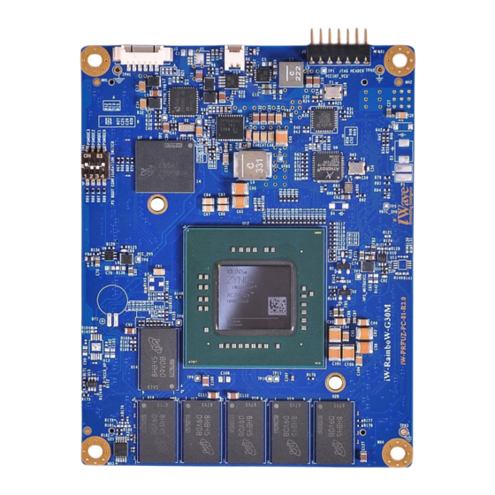
- Page 1 Zynq Ultrascale+ MPSoC SOM Hardware User Guide iW-RainboW-G30M Zynq Ultrascale+ MPSoC SOM Hardware User Guide REL1.0 iWave Systems Technologies Pvt. Ltd. Page 1 of 80...
- Page 2 If you are not the intended recipient (or authorized to receive for the recipient), you are hereby notified that any disclosure, copying distribution or use of any of the information contained within this document is STRICTLY PROHIBITED. Thank you. “iWave Systems Tech. Pvt. Ltd.” REL1.0 iWave Systems Technologies Pvt.
- Page 3 (including liability to any person by reason of negligence) will be accepted by iWave Systems, its subsidiaries or employees for any direct or indirect loss or damage caused by omissions from or inaccuracies in this document.
-
Page 4: Table Of Contents
2.8.1 PS Interfaces ............................49 2.8.1.1 PS-GTR High Speed Transceivers ..................... 49 2.8.1.2 Gigabit Ethernet Interface ......................50 2.8.1.3 USB2.0 OTG Interface ........................51 2.8.1.4 SD/SDIO Interface .......................... 51 2.8.1.5 SPI Interface ........................... 52 REL1.0 iWave Systems Technologies Pvt. Ltd. Page 4 of 80... - Page 5 3.2.4 Heat Sink ............................... 74 MechanicalCharacteristics ......................... 75 3.3.1 Zynq Ultrascale+ MPSoC SOM Mechanical Dimensions ................75 ORDERING INFORMATION ..........................77 APPENDIX ................................. 79 Zynq Ultrascale+ MPSoC SOM Development Platform ................79 REL1.0 iWave Systems Technologies Pvt. Ltd. Page 5 of 80...
- Page 6 Table 10: Power Input Requirement .......................... 70 Table 11: Power Sequence Timing ..........................71 Table 12: Power Consumption¹ ..........................72 Table 13: Temperature Specification ......................... 73 Table 14: Orderable Product Part Numbers ....................... 77 REL1.0 iWave Systems Technologies Pvt. Ltd. Page 6 of 80...
-
Page 7: Introduction
This document is the Hardware User Guide for the Zynq Ultrascale+ MPSoC System on Module based on the Xilinx Zynq Ultrascale+ MPSoC. This board is fully supported by iWave Systems Technologies Pvt. Ltd. This Guide provides detailed information on the overall design and usage of the Zynq Ultrascale+ MPSoC System on Module from a Hardware Systems perspective. - Page 8 System On Chip System On Module Serial Peripheral Interface UART Universal Asynchronous Receiver/Transmitter ULPI UTMI+ Low Pin Interface Universal Serial Bus USB OTG USB On The Go UTMI USB2.0 Transceiver Macrocell Interface REL1.0 iWave Systems Technologies Pvt. Ltd. Page 8 of 80...
-
Page 9: Terminlogy Description
Note: Signal Type does not include internal pull-ups or pull-downs implemented by the chip vendors and only includes the pull-ups or pull-downs implemented On-SOM. References • Zynq Ultrascale+ MPSoC Technical Reference Manual • Zynq Ultrascale+ MPSoC Device Overview REL1.0 iWave Systems Technologies Pvt. Ltd. Page 9 of 80... -
Page 10: Architecture And Design
SYSMONE4 supports 10bit 200KSPS ADC and supports upto 17 Analog Inputs (One dedicated Analog input and 16 auxiliary analog input from any PL BANKs) Figure 1: Zynq Ultrascale+ MPSoC SOM Block Diagram REL1.0 iWave Systems Technologies Pvt. Ltd. Page 10 of 80... -
Page 11: Zynq Ultrascale+ Mpsoc Som Features
• 1GB DDR4 SDRAM (16bit) for PL (Expandable) • 8GB eMMC Flash (Expandable) Other On-SOM Features • Gigabit Ethernet PHY Transceiver • USB2.0 Transceiver • JTAG Header • Fan Header REL1.0 iWave Systems Technologies Pvt. Ltd. Page 11 of 80... - Page 12 SD (4bit) x 1 Port • SPI x 1 Port • Debug UART x 1 Port • Data UART x 1 Port • I2C x 2 Ports • PS JTAG REL1.0 iWave Systems Technologies Pvt. Ltd. Page 12 of 80...
- Page 13 In Zynq Ultrascale+ MPSoC PS, GEM3 RGMII interface & USB1 ULPI interface signals are multiplexed in same pins and so either GEM3 or USB1 only can be supported. In Zynq Ultrascale+ MPSoC SOM, PL BANK45 & BANK46 supports variable IO voltage setting and configurable through software. REL1.0 iWave Systems Technologies Pvt. Ltd. Page 13 of 80...
-
Page 14: Zynq Ultrascale+ Mpsoc
Figure 2: Zynq Ultrascale+ MPSoC CPU Simplified Block Diagram Note: Please refer the latest Zynq Ultrascale+ MPSoC Datasheet & Technical Reference Manual for more details which may be revised from time to time. REL1.0 iWave Systems Technologies Pvt. Ltd. Page 14 of 80... -
Page 15: Figure 3: Zynq Ultrascale+ Mpsoc Devices Comparison
MPSoC to route most of the IO peripheral interfaces to PL Bank I/O pins referred as EMIO (Extended MIO). Zynq Ultrascale+ MPSoC’s PS Peripheral Pin mapping options between MIO & EMIO is shown below. REL1.0 iWave Systems Technologies Pvt. Ltd. Page 15 of 80... -
Page 16: Mpsoc Power
The I/O voltage of PL HD Banks (PL Bank 45 & 46) which are connected to Board to Board Connectors are generated from PMIC LDO3 and by default set to 1.8V. I/O voltage is configurable through software after bootup. REL1.0 iWave Systems Technologies Pvt. Ltd. Page 16 of 80... -
Page 17: Mpsoc Reset
I/O voltage of PL Bank45 is set between 1.8V to 3.3V. ² Mentioned voltage level is based on default I/O voltage set to PL Bank45. REL1.0 iWave Systems Technologies Pvt. Ltd. Page 17 of 80... -
Page 18: Mpsoc Configuration & Status
PMU. LED D5 is for PS_ERROR_STATUS and it indicates a secure lockdown state. Alternatively, it can be used by the PMU firmware to indicate system status. Figure 4: Error Status Indication LEDs REL1.0 iWave Systems Technologies Pvt. Ltd. Page 18 of 80... -
Page 19: Mpsoc Boot Mode Switch
Table 4: Boot Mode Switch Truth Table SW1 (4 Position Switch) Zynq Ultrascale+ MPSoC Boot Mode PS Mode 2 PS Mode 0 PS Mode 3 PS Mode 1 Switch Position Image PS JTAG eMMC (Default) USB0 REL1.0 iWave Systems Technologies Pvt. Ltd. Page 19 of 80... -
Page 20: Mpsoc System Monitor/Adc
The PMIC supports Real Time Clock functionality. It uses the Coin cell battery power from Board to Board Connector2 pin68 for RTC backup power. The PMIC can support backup battery charging to charge Lithium- Manganese coin cell batteries and super capacitors if required. REL1.0 iWave Systems Technologies Pvt. Ltd. Page 20 of 80... -
Page 21: Memory
The eMMC Flash size can be expandable up to maximum of 128GB based on the availability of higher density eMMC Flash device. Note: Refer ORDERING INFORMATION section for exact eMMC Flash size used on the SOM based on the Product Part Number. REL1.0 iWave Systems Technologies Pvt. Ltd. Page 21 of 80... -
Page 22: On Som Fearures
SOM as shown below. JTAG-HS2 Programming Cable can be directly connected to this JTAG Header. Number of Pins - 14 Connector Part - 877601416 from Molex Mating Connector - 0791077006 from Molex Figure 5: JTAG Header REL1.0 iWave Systems Technologies Pvt. Ltd. Page 22 of 80... -
Page 23: Table 5: Jtag Header Pinout
4.7K PU Power Ground. PS_JTAG_TDO PS_JTAG_TDO/ O, 1.8V LVCMOS JTAG Test Data Output. Power Ground. PS_JTAG_TDI PS_JTAG_TDI/ I, 1.8V LVCMOS/ JTAG Test Data Input. 4.7K PU Power Ground. Power Ground. REL1.0 iWave Systems Technologies Pvt. Ltd. Page 23 of 80... -
Page 24: Fan Header
Figure 6: Fan Header Table 6: Fan Header Pinout SoC Ball Name/ Signal Type/ Pin No Signal Name Description Pin Number Termination VCC_5V O, 5V Power Supply Voltage. Power Ground. REL1.0 iWave Systems Technologies Pvt. Ltd. Page 24 of 80... -
Page 25: Board To Board Connector1
Board Connector1 (J5) is physically located on bottom side of the SOM as shown below. Number of Pins - 240 Connector Part Number - QTH-120-01-L-D-A Mating Connector - QSH-120-01-L-D-A from Samtech Staking Height - 5mm Figure 7: Board to Board Connector1 REL1.0 iWave Systems Technologies Pvt. Ltd. Page 25 of 80... -
Page 26: Table 7: Board To Board Connector1 Pinout
PL_C16_LVDS45_L9N PL_K14_LVDS45_L2N GTHTXP2_223 PL_J16_LVDS45_L4P GTHTXN2_223 PL_H16_LVDS45_L4N PL_J14_LVDS45_L3N GTHTXP3_223 PL_J15_LVDS45_L3P GTHTXN3_223 PL_A14_LVDS46_L11P PL_A13_LVDS46_L11N GTHRXN3_223 PL_B12_LVDS46_L12P GTHRXP3_223 PL_A12_LVDS46_L12N GTHRXN2_223 PL_D17_LVDS45_L7N_HDGC GTHRXP2_223 PL_E17_LVDS45_L7P_HDGC PS_MGTRTXP0_505 GTREFCLK1P_223 PS_MGTRTXN0_505 GTREFCLK1N_223 PL_C14_LVDS46_L10P PL_B14_LVDS46_L10N PL_D12_LVDS46_L9P PS_MGTREFCLK0N_505 PL_C12_LVDS46_L9N PS_MGTREFCLK0P_505 REL1.0 iWave Systems Technologies Pvt. Ltd. Page 26 of 80... - Page 27 GTHTXP0_224 GTREFCLK0P_224 GTHTXN0_224 GTREFCLK0N_224 GTHTXP1_224 GTHTXN1_224 GTHRXN1_224 GTHRXP1_224 GTHRXN0_224 PL_F13_LVDS46_L5N_HDGC GTHRXP0_224 PL_G13_LVDS46_L5P_HDGC GTHTXP2_224 PL_F12_LVDS46_L6P_HDGC GTHTXN2_224 PL_E12_LVDS46_L6N_HDGC GTHTXP3_224 PL_E14_LVDS46_L7P_HDGC GTHTXN3_224 PL_E13_LVDS46_L7N_HDGC GTHRXN3_224 GTHRXP3_224 GTHRXN2_224 PL_C13_LVDS46_L8N_HDGC GTHRXP2_224 PL_D14_LVDS46_L8P_HDGC PS_MGTRTXP1_505 GTREFCLK1P_224 PS_MGTRTXN1_505 GTREFCLK1N_224 REL1.0 iWave Systems Technologies Pvt. Ltd. Page 27 of 80...
- Page 28 GTHTXN1_225 GEM3_TXD0/USB1_DIR(PS_MIO65 _502) GEM3_TXD1/USB1_DATA2(PS_MIO 66_502) GTHRXN1_225 GEM3_TXD2/USB1_NXT(PS_MIO67 _502) GTHRXP1_225 GEM3_TXD3/USB1_DATA0(PS_MIO 68_502) GTHRXN0_225 GTHRXP0_225 CAN0_RX(PS_MIO38_501) CAN0_TX(PS_MIO39_501) GEM3_TX_CTL/USB1_DATA1(PS_M IO69_502) CAN1_RX(PS_MIO41_501) GEM3_RX_CLK/USB1_STP(PS_MIO 70_502) CAN1_TX(PS_MIO40_501) GEM3_RX_CTL/USB1_DATA7(PS_M IO75_502) GTHTXP2_225 GTREFCLK1P_225 GTHTXN2_225 GTREFCLK1N_225 GTHTXP3_225 GEM3_RXD0/USB1_DATA3 (PS_MIO71_502) REL1.0 iWave Systems Technologies Pvt. Ltd. Page 28 of 80...
- Page 29 Zynq Ultrascale+ MPSoC SOM Hardware User Guide Signal Name B2B-1 Pin B2B-1 Pin Signal Name GTHTXN3_225 GEM3_RXD1/USB1_DATA4(PS_MIO 72_502) GEM3_RXD2/USB1_DATA5(PS_MIO 73_502) GTHRXN3_225 GEM3_RXD3/USB1_DATA6(PS_MIO 74_502) GTHRXP3_225 SOMPWR_EN GTHRXN2_225 GTHRXP2_225 REL1.0 iWave Systems Technologies Pvt. Ltd. Page 29 of 80...
-
Page 30: Ps Interfaces
In Zynq Ultrascale+ MPSoC SOM, the end user is responsible for sourcing the reference clocks to the PS-GTR lanes through Board to Board Connectors. This gives full flexibility to end user to select the required peripheral standards on PS-GTR lanes. REL1.0 iWave Systems Technologies Pvt. Ltd. Page 30 of 80... -
Page 31: Rgmii/Ulpi Interface
IEEE Standard for Ethernet (IEEE Std 802.3-2008). GEM controller supports MDIO interface for external PHY Management and it can be used through any PL Bank IOs through EMIO interface in SOM. REL1.0 iWave Systems Technologies Pvt. Ltd. Page 31 of 80... - Page 32 GEM3 RGMII Receive DATA2. Or TA5(PS_MIO73_502) USB1 ULPI Bi-Directional Data5. GEM3_RXD3/USB1_DA PS_MIO74_502/ I, 1.8V LVCMOS GEM3 RGMII Receive DATA3. Or TA6(PS_MIO74_502) USB1 ULPI Bi-Directional Data6. * Signal direction is mentioned considering GEM3 RGMII interface. REL1.0 iWave Systems Technologies Pvt. Ltd. Page 32 of 80...
-
Page 33: Can Interface
CAN0_RX(PS_MIO38_501) PS_MIO38_501/ I, 1.8V LVCMOS CAN0 Receive data. CAN0_TX(PS_MIO39_501) PS_MIO39_501/ O,1.8V LVCMOS CAN0 Transmit data. CAN1_RX(PS_MIO41_501) PS_MIO41_501/ I, 1.8V LVCMOS CAN1 Receive data. CAN1_TX(PS_MIO40_501) PS_MIO40_501/ O,1.8V LVCMOS CAN1 Transmit data. REL1.0 iWave Systems Technologies Pvt. Ltd. Page 33 of 80... -
Page 34: Interfaces
GTH Bank223 channel0 High speed differential transmitter positive. GTHTXN0_223 MGTHTXN0_223/ O, DIFF GTH Bank223 channel0 High speed differential transmitter negative. GTHRXN0_223 MGTHRXN0_223/ I, DIFF GTH Bank223 channel0 High speed differential receiver negative. REL1.0 iWave Systems Technologies Pvt. Ltd. Page 34 of 80... - Page 35 GTH Bank224 channel0 High speed differential transmitter positive. GTHTXN0_224 MGTHTXN0_224/ O, DIFF GTH Bank224 channel0 High speed differential transmitter negative. GTHRXN0_224 MGTHRXN0_224/ I, DIFF GTH Bank224 channel0 High speed differential receiver negative. REL1.0 iWave Systems Technologies Pvt. Ltd. Page 35 of 80...
- Page 36 GTH Bank225 channel0 High speed differential transmitter positive. GTHTXN0_225 MGTHTXN0_225/ O, DIFF GTH Bank225 channel0 High speed differential transmitter negative. GTHRXN0_225 MGTHRXN0_225/ I, DIFF GTH Bank225 channel0 High speed differential receiver negative. REL1.0 iWave Systems Technologies Pvt. Ltd. Page 36 of 80...
- Page 37 GTREFCLK0N_225 MGTREFCLK0N_225/ I, DIFF Bank225 differential reference clock0 negative. GTREFCLK1P_225 MGTREFCLK1P_225/ I, DIFF Bank225 differential reference clock1 positive. GTREFCLK1N_225 MGTREFCLK1N_225/ I, DIFF Bank225 differential reference clock1 negative. REL1.0 iWave Systems Technologies Pvt. Ltd. Page 37 of 80...
-
Page 38: Ios - Hd Bank45
Single ended I/O. PL_B16_LVDS45_L10N IO_L10N_AD10N_45/ IO, 1.8V LVDS PL Bank45 IO10 differential negative. Same pin can be configured as PLSYSMON differential analog input10 negative or Single ended I/O. REL1.0 iWave Systems Technologies Pvt. Ltd. Page 38 of 80... - Page 39 Single ended I/O. PL_K14_LVDS45_L2N IO_L2N_AD14N_45/ IO, 1.8V LVDS PL Bank45 IO2 differential negative. Same pin can be configured as PLSYSMON differential analog input14 negative or Single ended I/O. REL1.0 iWave Systems Technologies Pvt. Ltd. Page 39 of 80...
- Page 40 Single ended I/O. PL_F16_LVDS45_L6P_ IO_L6P_HDGC_45/ IO, 1.8V LVDS PL Bank45 IO6 differential positive. HDGC Same pin can be configured as HDGC Global Clock Input differential positive or Single ended I/O. REL1.0 iWave Systems Technologies Pvt. Ltd. Page 40 of 80...
-
Page 41: Ios - Hd Bank46
Single ended I/O. PL_A12_LVDS46_L12N IO_L12N_AD0N_46/ IO, 1.8V LVDS PL Bank46 IO12 differential negative. Same pin can be configured as PLSYSMON differential analog input0 negative or Single ended I/O. REL1.0 iWave Systems Technologies Pvt. Ltd. Page 41 of 80... - Page 42 Single ended I/O. PL_H14_LVDS46_L4P IO_L4P_AD8P_46/ IO, 1.8V LVDS PL Bank46 IO4 differential positive. Same pin can be configured as PLSYSMON differential analog input8 positive or Single ended I/O. REL1.0 iWave Systems Technologies Pvt. Ltd. Page 42 of 80...
- Page 43 IO, 1.8V LVDS PL Bank46 IO7 differential negative. HDGC N_46/E13 Same pin can be configured as HDGC Global Clock Input differential negative PLSYSMON differential analog input5 negative or Single ended I/O. REL1.0 iWave Systems Technologies Pvt. Ltd. Page 43 of 80...
-
Page 44: Power Control Input
215, 221, 227, 233, 239, 2, 8, 20, 26, 36, 54, 60, 62, 68, 80, 86, 96, 102, 114, 120, 122, 140, 146, 156, 162, 174, 180, 182, 188, 200, 206, 216, 222, 234, 240 REL1.0 iWave Systems Technologies Pvt. Ltd. Page 44 of 80... -
Page 45: Board To Board Connector2
Board Connector2 (J4) is physically located on bottom side of the SOM as shown below. Number of Pins - 240 Connector Part Number - QTH-120-01-L-D-A Mating Connector - QSH-120-01-L-D-A from Samtech Staking Height - 5mm Figure 8: Board to Board Connector2 REL1.0 iWave Systems Technologies Pvt. Ltd. Page 45 of 80... -
Page 46: Table 8: Board To Board Connector2 Pinout
GPHY_CTXRXP I2C0_SCL(PS_MIO10_500) UART1_TX(PS_MIO08_500) GPHY_BTXRXM UART1_RX(PS_MIO09_500) GPHY_BTXRXP UART0_TX(PS_MIO07_500) UART0_RX(PS_MIO06_500) GPHY_ATXRXM GPHY_LINK_LED2 GPHY_ATXRXP GPHY_ACTIVITY_LED1 SPI0_SCLK(PS_MIO0_500) SD1_DATA3(PS_MIO49_501) SPI0_SS0(PS_MIO3_500) SD1_DATA2(PS_MIO48_501) SPI0_MOSI(PS_MIO5_500) SD1_DATA1(PS_MIO47_501) SPI0_MISO(PS_MIO4_500) VRTC_3V0 SD1_DATA0(PS_MIO46_501) I2C1_SCL(PS_MIO24_500) SD1_CMD(PS_MIO50_501) SD1_CLK(PS_MIO51_501) PL_AE1_LVDS66_L20N PL_AA2_LVDS66_L24P PL_AD1_LVDS66_L20P PL_AA1_LVDS66_L24N PL_AA5_LVDS66_L18N PL_AC1_LVDS66_L23N REL1.0 iWave Systems Technologies Pvt. Ltd. Page 46 of 80... - Page 47 PL_AC18_LVDS64_L17N PL_AH18_LVDS64_L23N PL_AD19_LVDS64_L18P PL_AG16_LVDS64_L19P_DBC PL_AE19_LVDS64_L18N PL_AH16_LVDS64_L19N_DBC PL_AD5_LVDS66_L15P PL_AE14_LVDS64_L2P PL_AE5_LVDS66_L15N PL_AE13_LVDS64_L2N PL_AC2_LVDS66_L21N PL_AC14_LVDS64_L3P PL_AC3_LVDS66_L21P PL_AD14_LVDS64_L3N PL_AE18_LVDS64_L24P PL_AD15_LVDS64_L6P PL_AF18_LVDS64_L24N PL_AE15_LVDS64_L6N PL_AH17_LVDS64_L21P PL_AK13_LVDS64_L8P PL_AJ17_LVDS64_L21N PL_AK12_LVDS64_L8N PL_AJ16_LVDS64_L20P PL_AJ14_LVDS64_L9P PL_AK16_LVDS64_L20N PL_AK14_LVDS64_L9N PL_AK17_LVDS64_L22P_DBC PL_AB15_LVDS64_L5N PL_AK18_LVDS64_L22N_DBC PL_AA15_LVDS64_L5P REL1.0 iWave Systems Technologies Pvt. Ltd. Page 47 of 80...
- Page 48 GTHRXN0_226 GTREFCLK0N_226 GTHTXP0_226 GTHRXP3_226 GTHTXN0_226 GTHRXN3_226 GTHRXP1_226 GTHTXP3_226 GTHRXN1_226 GTHTXN3_226 GTHTXP1_226 PS_MGTRRXP3_505 GTHTXN1_226 PS_MGTRRXN3_505 GTHRXP2_226 PS_MGTRTXP3_505 GTHRXN2_226 PS_MGTRTXN3_505 GTHTXP2_226 PS_MGTREFCLK3P_505 GTHTXN2_226 PS_MGTREFCLK3N_505 GTREFCLK1P_226 GTREFCLK1N_226 PS_MGTRRXP2_505 PS_MGTREFCLK2P_505 PS_MGTRRXN2_505 PS_MGTREFCLK2N_505 PS_MGTRTXP2_505 PS_MGTRTXN2_505 REL1.0 iWave Systems Technologies Pvt. Ltd. Page 48 of 80...
-
Page 49: Ps Interfaces
PS_MGTRRXN3_505/ I, DIFF PS-GTR Lane3 High speed differential receiver negative. PS_MGTREFCLK3P_505 PS_MGTREFCLK3P_505/ I, DIFF PS-GTR Lane3 differential reference clock positive. PS_MGTREFCLK3N_505 PS_MGTREFCLK3N_505/ I, DIFF PS-GTR Lane3 differential reference clock negative. REL1.0 iWave Systems Technologies Pvt. Ltd. Page 49 of 80... -
Page 50: Gigabit Ethernet Interface
Gigabit Ethernet differential pair 1 positive. GPHY_LINK_LED2 O, 2.5V CMOS/ Gigabit Ethernet 1000Mbps Link status 10K PD LED (Active High). GPHY_ACTIVITY_LED1 O, 2.5V CMOS/ Gigabit Ethernet Activity LED (Active 10K PD High). REL1.0 iWave Systems Technologies Pvt. Ltd. Page 50 of 80... -
Page 51: Usb2.0 Otg Interface
Speed mode (50Mhz), SDR12 (25Mhz), SDR25 (25Mhz), SDR50 (100Mhz), SDR104 (200Mhz) & DDR50 mode (50Mhz). Also in SD mode, data transfers in 1-bit and 4-bit modes. The Zynq Ultrascale+ MPSoC SOM supports Card Detect, Write Protect & Power Enable/Voltage Select pins through MIO pins. REL1.0 iWave Systems Technologies Pvt. Ltd. Page 51 of 80... -
Page 52: Spi Interface
B2B Connector1 SoC Ball Name/ Signal Type/ Description Pin No Pin Name Pin Number Termination SPI0_SS2(PS_MIO1_500) PS_MIO1_500/ I/O, 1.8V LVCMOS SPI chip select2. Same pin can be configured as GPIO. REL1.0 iWave Systems Technologies Pvt. Ltd. Page 52 of 80... -
Page 53: Debug Uart Interface
Signal Type/ Description Pin No Pin Name Pin Number Termination UART1_TX(PS_MIO08 PS_MIO8_500/ O, 1.8V LVCMOS UART1 Transmit data line. _500) UART1_RX(PS_MIO09 PS_MIO9_500/ I, 1.8V LVCMOS UART1 Receive data line. _500) REL1.0 iWave Systems Technologies Pvt. Ltd. Page 53 of 80... -
Page 54: I2C Interface
JTAG Test Data Input. 4.7K PS_JTAG_TMS PS_JTAG_TMS/ I, 1.8V LVCMOS/ JTAG Test Mode Select. 4.7K PS_JTAG_TCK PS_JTAG_TCK/ I, 1.8V LVCMOS/ JTAG Test Clock. 4.7K PS_JTAG_TDO PS_JTAG_TDO/ O, 1.8V LVCMOS JTAG Test Data Output. REL1.0 iWave Systems Technologies Pvt. Ltd. Page 54 of 80... -
Page 55: Interfaces
GTH Bank226 channel2 High speed differential transmitter positive. GTHTXN2_226 MGTHTXN2_226/ O, DIFF GTH Bank226 channel2 High speed differential transmitter negative. GTHRXP3_226 MGTHRXP3_226/ I, DIFF GTH Bank226 channel3 High speed differential receiver positive. REL1.0 iWave Systems Technologies Pvt. Ltd. Page 55 of 80... - Page 56 GTREFCLK0N_226 MGTREFCLK0N_226/ I, DIFF Bank226 differential reference clock0 negative. GTREFCLK1P_226 MGTREFCLK1P_226/ I, DIFF Bank226 differential reference clock1 positive. GTREFCLK1N_226 MGTREFCLK1N_226/ I, DIFF Bank226 differential reference clock1 negative. REL1.0 iWave Systems Technologies Pvt. Ltd. Page 56 of 80...
-
Page 57: Ios - Hp Bank64
Same pin can be configured as Single ended I/O. PL_AH17_LVDS64_L2 IO_L21P_T3L_N4_AD IO, 1.8V LVDS PL Bank64 IO21 differential positive. 8P_64/AH17 Same pin can be configured as PLSYSMON differential analog input8 positive or Single ended I/O. REL1.0 iWave Systems Technologies Pvt. Ltd. Page 57 of 80... - Page 58 Single ended I/O. PL_AG15_LVDS64_L1 IO_L12N_T1U_N11_ IO, 1.8V LVDS PL Bank64 IO12 differential negative. 2N_GC GC_64/AG15 Same pin can be configured as GC Global Clock Input differential negative or Single ended I/O. REL1.0 iWave Systems Technologies Pvt. Ltd. Page 58 of 80...
- Page 59 Same pin can be configured as PLSYSMON differential analog input9 negative or Single ended I/O. PL_AE14_LVDS64_L2P IO_L2P_T0L_N2_64/ IO, 1.8V LVDS PL Bank64 IO2 differential positive. AE14 Same pin can be configured as Single ended I/O. REL1.0 iWave Systems Technologies Pvt. Ltd. Page 59 of 80...
- Page 60 Single ended I/O. PL_AB15_LVDS64_L5 IO_L5N_T0U_N9_AD IO, 1.8V LVDS PL Bank64 IO5 differential negative. 14N_64/AB15 Same pin can be configured as PLSYSMON differential analog input14 negative or Single ended I/O. REL1.0 iWave Systems Technologies Pvt. Ltd. Page 60 of 80...
- Page 61 Single ended I/O. PL_AB16_LVDS64_L16 IO_L16N_T2U_N7_Q IO, 1.8V LVDS PL Bank64 IO16 differential negative. N_QBC BC_AD3N_64/AB16 Same pin can be configured as PLSYSMON differential analog input3 negative or Single ended I/O. REL1.0 iWave Systems Technologies Pvt. Ltd. Page 61 of 80...
-
Page 62: Ios -Hp Bank66
Single ended I/O. PL_AB10_LVDS66_L5P IO_L5P_T0U_N8_AD IO, 1.8V LVDS PL Bank66 IO5 differential positive. 14P_66/AB10 Same pin can be configured as PLSYSMON differential analog input14 positive or Single ended I/O. REL1.0 iWave Systems Technologies Pvt. Ltd. Page 62 of 80... - Page 63 Same pin can be configured as Single ended I/O. PL_AB6_LVDS66_L14P IO_L14P_T2L_N2_GC IO, 1.8V LVDS PL Bank66 IO14 differential positive. _66/AB6 Same pin can be configured as GC Global Clock Input differential positive or Single ended I/O. REL1.0 iWave Systems Technologies Pvt. Ltd. Page 63 of 80...
- Page 64 6/AC1 Same pin can be configured as Single ended I/O. PL_AB1_LVDS66_L23P IO_L23P_T3U_N8_66 IO, 1.8V LVDS PL Bank66 IO23 differential positive. /AB1 Same pin can be configured as Single ended I/O. REL1.0 iWave Systems Technologies Pvt. Ltd. Page 64 of 80...
- Page 65 Single ended I/O. PL_AD9_LVDS66_L7N IO_L7N_T1L_N1_QB IO, 1.8V LVDS PL Bank66 IO7 differential negative. _QBC C_AD13N_66/AD9 Same pin can be configured as PLSYSMON differential analog input13 negative or Single ended I/O. REL1.0 iWave Systems Technologies Pvt. Ltd. Page 65 of 80...
- Page 66 Single ended I/O. PL_AC3_LVDS66_L21P IO_L21P_T3L_N4_AD IO, 1.8V LVDS PL Bank66 IO21 differential positive. 8P_66/AC3 Same pin can be configured as PLSYSMON differential analog input8 positive or Single ended I/O. REL1.0 iWave Systems Technologies Pvt. Ltd. Page 66 of 80...
-
Page 67: Power & Reset Input
174, 180, 186, 192, 198, 204, 210, 216, 222, 228, 234, 240 VRTC_3V0 I, 3V Power 3V backup coin cell input for RTC. RESET_SW_IN PS_SRST_B/ I, 1.8V LVCMOS/ Active low reset input. 4.7K PU REL1.0 iWave Systems Technologies Pvt. Ltd. Page 67 of 80... -
Page 68: Zynq Ultrascale+ Mpsoc Ps Pin Multiplexing On Board To Board Connectors
I2C1_SCL PJTAG_TDO SPI1_SS1 UART1_TX USB0_DATA4 PS_MIO61_502 GPIO61 GEM2_RXD2 CAN1_RX I2C1_SDA PJTAG_TMS SPI1_SS0 UART1_RX USB0_DATA5 PS_MIO62_502 GPIO62 GEM2_RXD3 CAN0_RX I2C0_SCL SPI1_MISO UART0_RX USB0_DATA6 PS_MIO63_502 GPIO63 GEM2_RX_CTL CAN0_TX I2C0_SDA SPI1_MIOSI UART0_TX USB0_DATA7 REL1.0 iWave Systems Technologies Pvt. Ltd. Page 68 of 80... - Page 69 UART0_TX PS_MIO10_500 GPIO10 NFC_RB_N CAN0_RX I2C0_SCL SPI1_MISO UART0_RX GPIOs/I2C1 PS_MIO25_500 GPIO25 NFC_RE_N CAN1_RX I2C1_SDA UART1_RX PS_MIO24_500 GPIO24 NFC_DATA7 CAN1_TX I2C1_SCL UART1_TX PS_JTAG_TDI PS_JTAG_TDI JTAG PS_JTAG_TMS PS_JTAG_TMS PS_JTAG_TCK PS_JTAG_TCK PS_JTAG_TDO PS_JTAG_TDO REL1.0 iWave Systems Technologies Pvt. Ltd. Page 69 of 80...
-
Page 70: Technical Specification
² Zynq Ultrascale+ MPSoC SOM uses this voltage as backup power source to PMIC RTC when VCC_5V is off. This is an optional power and required only if RTC functionality is used. REL1.0 iWave Systems Technologies Pvt. Ltd. Page 70 of 80... -
Page 71: Power Input Sequencing
VCC_5V rise time to SOMPWR_EN rise time ≥ 0 ms SOMPWR_EN fall time to VCC_5V fall time ≥ 0 ms VCC_5V fall time to VRTC_3V0 fall time ≥ 0 ms REL1.0 iWave Systems Technologies Pvt. Ltd. Page 71 of 80... -
Page 72: Power Consumption
(XPE) tool to find the exact power of the MPSoC device based on the PS/PL design requirement and add the safe margin of 3A (@ VCC_5V) for other components power in the SOM (such as maximum DDR4 , eMMC etc..). REL1.0 iWave Systems Technologies Pvt. Ltd. Page 72 of 80... -
Page 73: Environmental Characteristics
3.2.3 Electrostatic Discharge iWave’s Zynq Ultrascale+ MPSoC SOM is sensitive to electro static discharge and so high voltages caused by static electricity could damage some of the devices on board. It is packed with necessary protection while shipping. Do not open or use the SOM except at an electrostatic free workstation. -
Page 74: Heat Sink
CPU. iWave supports Heat Sink Solution for Zynq Ultrascale+ MPSoC SOM. Please refer the below figure for Heat Sink dimension details. For Heat Sink ordering information, please refer section 4 ORDERING INFORMATION. -
Page 75: Mechanicalcharacteristics
Zynq Ultrascale+ MPSoC SOM PCB size is 95mm x 75mm x 1.5mm. SOM mechanical dimension is shown below. Figure 11: Mechanical dimension of Zynq Ultrascale+ MPSoC SOM - Top View REL1.0 iWave Systems Technologies Pvt. Ltd. Page 75 of 80... -
Page 76: Figure 12: Mechanical Dimension Of Zynq Ultrascale+ Mpsoc Som - Bottom View
Connectors (4.27mm) followed by Bulk capacitors (2.5mm). Please refer the below figure which gives height details of the Zynq Ultrascale+ MPSoC SOM. Figure 13: Mechanical dimension of Zynq Ultrascale+ MPSoC SOM - Side View REL1.0 iWave Systems Technologies Pvt. Ltd. Page 76 of 80... -
Page 77: Ordering Information
The below table provides the standard orderable part numbers for different Zynq Ultrascale+ MPSoC SOM variations. Please contact iWave for orderable part number of higher RAM memory size or Flash memory size SOM configurations. Also if the desired part number is not listed in below table or if any custom configuration part number is required, please contact iWave. - Page 78 Heat Sink for Zynq Ultrascale+ MPSoC SOM Important Note: Some of the above-mentioned Part Number is subject to MOQ purchase. Please contact iWave for further details. Note: For SOM identification purpose, Product Part Number and SOM Unique Serial Number are pasted as Label with Barcode readable format on SOM.
-
Page 79: Appendix
Systems supports iW-RainboW-G30D – Zynq Ultrascale+ MPSoC SOM Development Platform which is targeted for quick validation of Zynq Ultrascale+ MPSoC based SOM. iWave's Zynq Ultrascale+ MPSoC Development Board incorporates Zynq Ultrascale+ MPSoC SOM and High performance Carrier board with complete BSP support. - Page 80 Zynq Ultrascale+ MPSoC SOM Hardware User Guide REL1.0 iWave Systems Technologies Pvt. Ltd. Page 80 of 80...
Need help?
Do you have a question about the Zynq Ultrascale+ iW-RainboW-G30M and is the answer not in the manual?
Questions and answers