Table of Contents

Related Manuals for iWave iW-RainboW-G25D


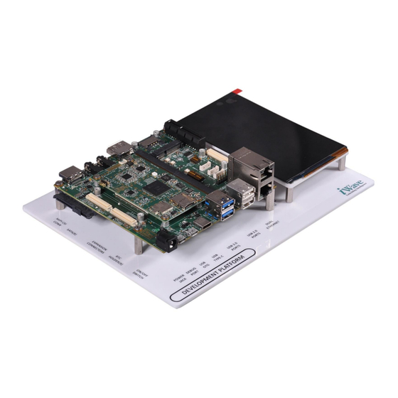
Summary of Contents for iWave iW-RainboW-G25D
- Page 1 Snapdragon 820 SMARC Development Platform Hardware User Guide iW-RainboW-G25D Snapdragon 820 SMARC Development Platform Hardware User Guide DRAFT VERSION SUBJECT TO CHANGE REL0.1 iWave Systems Technologies Pvt. Ltd. Page 1 of 61...
- Page 2 If you are not the intended recipient (or authorized to receive for the recipient), you are hereby notified that any disclosure, copying distribution or use of any of the information contained within this document is STRICTLY PROHIBITED. Thank you. “iWave Systems Tech. Pvt. Ltd.” REL0.1 iWave Systems Technologies Pvt.
- Page 3 No warranty of accuracy is given concerning the contents of the information contained in this publication. To the extent permitted by law no liability (including liability to any person by reason of negligence) will be accepted by iWave Systems, its subsidiaries or employees for any direct or indirect loss or damage caused by omissions from or inaccuracies in this document.
-
Page 4: Table Of Contents
3.2.1 Environmental Specification ........................57 3.2.2 RoHS Compliance ............................57 3.2.3 Electrostatic Discharge ..........................57 Mechanical Characteristics ..........................58 3.3.1 Snapdragon 820 SMARC SOM Mechanical Dimensions ................58 ORDERING INFORMATION .......................... 60 REL0.1 iWave Systems Technologies Pvt. Ltd. Page 4 of 61... - Page 5 Table 11: Expansion Connector1 Pin Out........................50 Table 12: Expansion Connector2 Pin Out........................53 Table 13: Power Input Requirement ..........................57 Table 14: Environmental Specification ........................... 57 Table 15: Orderable Product Part Numbers ........................60 REL0.1 iWave Systems Technologies Pvt. Ltd. Page 5 of 61...
-
Page 6: Introduction
This document is the Hardware User Guide for the Snapdragon 820 SMARC Development platform “iW-RainboW- G25D” based on the Qualcomm APQ8096 Application processor. This board is fully supported by iWave Systems Technologies Pvt. Ltd. This Guide provides detailed information on the overall design and usage of the Snapdragon 820 APQ8096 based SMARC development platform from a Hardware Systems perspective. - Page 7 Secure Digital SDRAM Synchronous Dynamic Random Access Memory SMARC SOM Smart Mobility ARChitecture To Be Defined UART Universal Asynchronous Receiver/Transmitter Universal Serial Bus USB OTG USB On The Go Voltage REL0.1 iWave Systems Technologies Pvt. Ltd. Page 7 of 61...
-
Page 8: Terminlogy Description
Note: Signal Type does not include internal pull-ups or pull-downs implemented by the chip vendors and only includes the pull-ups or pull-downs implemented On-SMARC SOM. References • APQ8096 Hardware User Manuals. • APQ8096 SMARC SOM Hardware User Manual • SMARC Specification V2.0 REL0.1 iWave Systems Technologies Pvt. Ltd. Page 8 of 61... -
Page 9: Architecture And Design
This section provides detailed information about the Snapdragon 820 SMARC SOM features and Hardware architecture with high level block diagram. Snapdragon 820 SMARC SOM Block Diagram iW-RainboW-G25D Snapdragon 820 SMARC DevKit Block Diagram To On-board APQ8096 SMARC Edge Connector On-Board... -
Page 10: Snapdragon 820 Smarc Som Features
• M.2 Connector (Optional) A&V Expansion Connector • MIPI CSI - 4 lanes x 1 Port • MIPI CSI - 4 lanes x 1 Port • I2S/HDA x 1 Port REL0.1 iWave Systems Technologies Pvt. Ltd. Page 10 of 61... - Page 11 SLIMBUS x 1 Port • Audio Code Inputs and Outputs (Optional) • GPIO General Specification • Power Supply : 12V, 2A Power Input Jack • Form Factor : 120mm X 120mm Nano ITX REL0.1 iWave Systems Technologies Pvt. Ltd. Page 11 of 61...
-
Page 12: Smarc Mxm Connector
This standard 314-pin robust connector is capable of handling high-speed serialized signals and can be used for size constrained embedded applications. This SMARC MXM Edge mating connector (J16) is physically located at the top of the board as shown below. Figure 2: SMARC MXM Connector REL0.1 iWave Systems Technologies Pvt. Ltd. Page 12 of 61... -
Page 13: Table 3: Smarc Mxm Connector Pin Out
Gigabit Ethernet link status GBE0_LINK1000# I, 3.3V CMOS Gigabit Ethernet MDI GBE0_MDI2- GBE0_MDI2- IO, DIFF differential pair 2 negative. Gigabit Ethernet MDI GBE0_MDI2+ GBE0_MDI2+ IO, DIFF differential pair 2 positive. REL0.1 iWave Systems Technologies Pvt. Ltd. Page 13 of 61... - Page 14 SPI0_CS0# I, 1.8V CMOS SPI0 Chip Select 0 N(GPIO_2) BLSP1_SPI_CLK( GPIO_3/ SPI0_CK I, 1.8V CMOS SPI0 Clock GPIO_3) BLSP1_SPI_MIS GPIO_1/ SPI0_DIN O, 1.8V CMOS SPI0 Master IN Slave Out O(GPIO_1) REL0.1 iWave Systems Technologies Pvt. Ltd. Page 14 of 61...
- Page 15 Note: Connected to USB USB Port1 Data Negative USB_HUB3OUT_ USB1- IO, DIFF Note: Connected to USB USB Port1 Power Enable/ Over Current Indicator USB1_EN_OC# USB_HUB3_OC IO, 3.3V CMOS Note: Connected to USB REL0.1 iWave Systems Technologies Pvt. Ltd. Page 15 of 61...
- Page 16 PCIE0_REFCLK_M Power Ground. PCIE1_REFCLK_ PCIE1_REFCLK_P/ PCIE_A_REFCK+ I, Diff PCIE1 Clock Positive PCIE1_REFCLK_ PCIE1_REFCLK_M/ PCIE_A_REFCK- I, Diff PCIE1 Clock Negative Power Ground. PCIE1_RX_P/ PCIE_A_RX+ PCIE1_RX_P O, Diff PCIE1 Receive Positive REL0.1 iWave Systems Technologies Pvt. Ltd. Page 16 of 61...
- Page 17 GPIO1 / SMARC_GPIO_1 GPIO_89/ SMARC General Purpose P109 IO, 1.8V CMOS CAM1_PWR# (GPIO_89) Input/output 1 SMARC_GPIO_2 GPIO_97/ SMARC General Purpose P110 GPIO2 / CAM0_RST# IO, 1.8V CMOS (GPIO_97) AR49 Input/output 2 REL0.1 iWave Systems Technologies Pvt. Ltd. Page 17 of 61...
- Page 18 I, 1.8V CMOS BLSP9_UART Transmitter (GPIO_49) BE49 BLSP9_UART_R GPIO_50/ P130 SER0_RX O, 1.8V CMOS BLSP9_UART Receiver X(GPIO_50) BE51 BLSP9_UART_RF GPIO_52/ BLSP9_UART Request to P131 SER0_RTS# I, 1.8V CMOS R_N(GPIO_52) BD50 Send REL0.1 iWave Systems Technologies Pvt. Ltd. Page 18 of 61...
- Page 19 VDD_IN CSI1_TX+ / CCI_I2C1_SCL(G GPIO_20/ I, 1.8V CMOS MIPI CSI1 I2C Clock I2C_CAM1_CK PIO_20) CSI1_TX- / CCI_I2C1_SDA(G GPIO_19/ IO, 1.8V CMOS MIPI CSI1 I2C Data I2C_CAM1_DAT PIO_19) Power Ground. RSVD1 REL0.1 iWave Systems Technologies Pvt. Ltd. Page 19 of 61...
- Page 20 GBE1_LINK100# GBE1_MDI1+ GBE1_MDI1- GBE1_LINK1000# GBE1_MDI2+ GBE1_MDI2- Power Ground. GBE1_MDI3+ GBE1_MDI3- GBE1_CTREF PCIE_D_TX+ PCIE_D_TX- GBE1_LINK_ACT# PCIE_D_RX+ PCIE_D_RX- Power Ground. USB Port4 Data Positive USB_HUB4OUT_ USB4+ IO, DIFF Note: Connected to USB REL0.1 iWave Systems Technologies Pvt. Ltd. Page 20 of 61...
- Page 21 HDA_SDI / I2S2_SDIN O, 1.8V CMOS I2S Channel1 Data Input O_77) MI2S_3_SCK(GP GPIO_75/ HDA_CK / I2S2_CK I, 1.8V CMOS I2S Channel1 Clock IO_75) SATA_ACT# USB5_EN_OC# ESPI_IO_2 ESPI_IO_3 ESPI_RESET# USB5+ USB5- Power Ground. REL0.1 iWave Systems Technologies Pvt. Ltd. Page 21 of 61...
- Page 22 Note: Connected to USB Power Ground. USB3.0 Port2 Receive USB3_HUB1_RX Positive USB2_SSRX+ O, DIFF Note: Connected to USB USB3.0 Port2 Receive USB3_HUB1_RX Negative USB2_SSRX- O, DIFF Note: Connected to USB REL0.1 iWave Systems Technologies Pvt. Ltd. Page 22 of 61...
- Page 23 Note: Optionally connected to PCIE2_RX_P PCIE_B_RX- Note: Optionally connected to PCIE2_RX_M Power Ground. PCIE_B_TX+ Note: Optionally connected to PCIE2_TX_P PCIE_B_TX- Note: Optionally connected to PCIE2_TX_M Power Ground. DP0_LANE0+ DP0_LANE0- DP0_AUX_SEL REL0.1 iWave Systems Technologies Pvt. Ltd. Page 23 of 61...
- Page 24 / I, DIFF BE29 lane 2 positive DSI1_D2+ LVDS1_2- / MIPI_DSI1_LN2 MIPI_DSI1_LN2_N/ MIPI DSI1 differential data S118 eDP1_TX2- / I, DIFF BD28 lane 2 negative DSI1_D2- S119 Power Ground. REL0.1 iWave Systems Technologies Pvt. Ltd. Page 24 of 61...
- Page 25 MIPI DSI0 differential clock S134 eDP0_AUX+ / I, DIFF BF34 positive DSI0_CLK+ LVDS0_CK- / MIPI_DSI0_CLK_ MIPI_DSI0_CLK_N/ MIPI DSI0 differential clock S135 eDP0_AUX- / I, DIFF BE33 negative DSI0_CLK- S136 Power Ground. REL0.1 iWave Systems Technologies Pvt. Ltd. Page 25 of 61...
- Page 26 O, 1.8V CMOS S153 CARRIER_STBY# CARRIER_STBY# enabled only after 10K PU CARRIER_STBY# goes High. Carrier power should be CARRIER_PWR_ I, 1.8V CMOS enabled only after S154 CARRIER_PWR_ON 10K PU CARRIER_PWR_ON goes High REL0.1 iWave Systems Technologies Pvt. Ltd. Page 26 of 61...
- Page 27 USB0 operates in Client Mode when in the Force Recovery function invoked. S156 BATLOW# O, 1.8V CMOS Module vendor specific S157 TEST# TEST# 10K PU test is not supported. S158 Power Ground. REL0.1 iWave Systems Technologies Pvt. Ltd. Page 27 of 61...
-
Page 28: On Board Switches
SMARC Carrier board has seven Switches on Top side of carrier card to support generic SAMRC features. All the seven switches location is highlight in below image and the switch description is given in the following table. Figure 3: SMARC On Board Switches REL0.1 iWave Systems Technologies Pvt. Ltd. Page 28 of 61... -
Page 29: Table 4: Board Configuration Switch
SW4 LID# Not Supported SLEEP# Not Supported (DIP SW) BATLOW# Not Supported TEST# Not Supported Carrier Power ON/ Carrier Power is Carrier Power is ON (Toggle SW) OFF Switch REL0.1 iWave Systems Technologies Pvt. Ltd. Page 29 of 61... -
Page 30: Serial Interface Features
FT232RQ is connected to USB Micro AB Connector (J22). This USB Micro AB Connector can be used for Debug purpose which is physically located at the top of the board as shown below. Figure 4: Debug UART REL0.1 iWave Systems Technologies Pvt. Ltd. Page 30 of 61... -
Page 31: Data Uart Header
3.3V Supply Voltage. UART_RXD BLSP9_UART_RX(GPIO_50) I, 3.3V CMOS SCIFB1 interface Receive signal. UART_TXD BLSP9_UART_TX(GPIO_49) O, 3.3V CMOS SCIFB1 interface Transmit signal. UART_RTS# BLSP9_UART_RFR_N(GPIO_52) I, 3.3V CMOS SCIFB1 interface Ready To Send signal. REL0.1 iWave Systems Technologies Pvt. Ltd. Page 31 of 61... -
Page 32: High Speed Interface Features
Board configuration switch (SW1) is set to OFF position, then PCIe channel A of SAMRC MXM connector is connected to PCIex4 connector which is physically located at the top of the board as shown below. Figure 6: PCIex4 Connector REL0.1 iWave Systems Technologies Pvt. Ltd. Page 32 of 61... -
Page 33: Table 6: Pciex4 Connector Pin Out
Ground. PCIE0_RX- PCIEA_RX- I, DIFF PCIe Port 0 Receive pair negative. PRSNT2# Power Ground. Power Ground. RSVD NC, Reserved Pin. PCIE1_TX+ PCIEB_TX+ O, DIFF PCIe Port 1 Transmit pair positive. REL0.1 iWave Systems Technologies Pvt. Ltd. Page 33 of 61... - Page 34 NC, PCIe Port 3 Receive pair positive. Power Ground. PCIE3_RX- NC, PCIe Port 3 Receive pair negative. RSVD NC, Reserved Pin. Power Ground. PRSNT3# RSVD NC, Reserved Pin. Power Ground. REL0.1 iWave Systems Technologies Pvt. Ltd. Page 34 of 61...
-
Page 35: Figure 7: Mini Pcie Connector
COEX2 1.5V VCC_1V5 O, 1.5V Power 1.5V Supply Voltage. CLK_REQ# CLK_REQ# O, 3.3V CMOS Used to enable Clock. UIM_PWR Power Ground. UIM_DATA REFCLK- PCIe_REFCLK_DM O, DIFF PCIe Clock positive. UIM_CLK REL0.1 iWave Systems Technologies Pvt. Ltd. Page 35 of 61... - Page 36 O, 3.3V CMOS Connected to D3 Green LED cathode. RESERVED 1.5V VCC_1V5 O, 1.5V Power 1.5V Supply Voltage. RESERVED Power Ground. RESERVED +3.3V_aux VPCIe_3V3 O, 3.3V Power 3.3V Supply Voltage. REL0.1 iWave Systems Technologies Pvt. Ltd. Page 36 of 61...
-
Page 37: Usb3.0 Host
SMARC MXM connector USB2 and USB3 ports. This USB3.0 connector is physically located at the top of the board as shown below. Figure 8: USB3.0 Host REL0.1 iWave Systems Technologies Pvt. Ltd. Page 37 of 61... -
Page 38: Communication Interface Features
SMARC MXM connector is directly connected to RJ45 Magjack (J6, Bottom). Also, it supports Speed (Yellow) and Link/Activity (Green) LED indications on RJ45 Magjack. This RJ45 Magjack combo connector is physically located at the top of the board as shown below. Figure 9: RJ45 Magjack REL0.1 iWave Systems Technologies Pvt. Ltd. Page 38 of 61... -
Page 39: Usb2.0 Host
SMARC MXM connector USB1 and USB4 ports. This USB3.0 connector is physically located at the top of the board as shown below. Figure 10: USB2.0 Host Port REL0.1 iWave Systems Technologies Pvt. Ltd. Page 39 of 61... -
Page 40: Usb2.0 Otg
USB0_EN_OC# should drive low to disable the power to the connector. This USB2.0 OTG connector is physically located at the top of the board as shown below. Figure 11: USB2.0 OTG REL0.1 iWave Systems Technologies Pvt. Ltd. Page 40 of 61... -
Page 41: Sdio Port
Dolby Digital Plus, Dolby True-HD, and DTS-HD Master. HDMI Signals from the SMARC connector is connected to Standard HDMI connector with ESD protection circuitry. HDMI Output connector (J23) is physically located on top of the board as shown below. Figure 12: HDMI Output REL0.1 iWave Systems Technologies Pvt. Ltd. Page 41 of 61... -
Page 42: Mipi Dsi Display
SMARC MXM connector is used for this LCD interface. This MIPI_DSI0 interface signals are connected Display connector (J1) via EMI protection circuit and is physically located at the top of board as shown below. Figure 13: MIPI Display Connector REL0.1 iWave Systems Technologies Pvt. Ltd. Page 42 of 61... -
Page 43: Table 8: Mipi Display Connector Pin Out
O, 1,8V CMOS I2C Clock for Capacitive Touch TP_SCL I2C_LCD_CK O, 1,8V CMOS RESET for Capacitive Touch TP_RESET TR1_RST I 1,8V CMOS Interrupt from Capacitive Touch TP_INT GPIO_7_TP_INT1 Power Ground. REL0.1 iWave Systems Technologies Pvt. Ltd. Page 43 of 61... -
Page 44: Mipi Csi Camera
Camera interface. This MIPI_CSI0 interface signals are connected Display connector (J1) via EMI protection circuit and is physically located at the top of board as shown below. Figure 14: MIPI Camera Connector REL0.1 iWave Systems Technologies Pvt. Ltd. Page 44 of 61... -
Page 45: Table 9: Mipi Camera Connector Pin Out
MIPI_CSI DATA Lane0 Positive MDP0 MD0_RX0+ I, Diff MIPI_CSI DATA Lane0 Negative MDN0 MD0_RX0- Power Ground. DGND I, Diff MIPI_CSI Clock Positive MD0_CK+ I, Diff MIPI_CSI Clock Negative MD0_CK- Power Ground. DGND REL0.1 iWave Systems Technologies Pvt. Ltd. Page 45 of 61... -
Page 46: Audio & Video Expansion Connector
Audio & Video Expansion connector is physically located at the top of board as shown below. Connectors Part number: DF17(3.0)-80DS-0.5V(57) from Hirose Mating Connector : DF17(2.0)-80DP-0.5V(57) from Hirose Audio & Video Expansion connector Figure 15: REL0.1 iWave Systems Technologies Pvt. Ltd. Page 46 of 61... -
Page 47: Table 10: Audio & Video Expansion Connector Pin Out
MIPI DSI1 differential data lane 1 negative HDA_SYNC/I2S2_LRCK O, 1.8V CMOS I2S /HAD Left Right Synchronise clock LVDS1_1+/DSI1_D1+ O, DIFF MIPI DSI1 differential data lane 1 Positive Power Ground. Power Ground. RSVD6 REL0.1 iWave Systems Technologies Pvt. Ltd. Page 47 of 61... - Page 48 Camera I2C Clock CSI1_CK- I, DIFF MIPI CSI1 differential Clock negative GPIO_3_CAM1_XSHD IO, 1.8V CMOS General Purpose Input / Output CSI1_CK+ I, DIFF MIPI CSI1 differential Clock Positive Power Ground. REL0.1 iWave Systems Technologies Pvt. Ltd. Page 48 of 61...
-
Page 49: Carrier Expansion Connector
Expansion connectors are physically located at the top of board as shown below. Connectors Part number: DF17(3.0)-80DS-0.5V(57) from Hirose Mating Connector : DF17(2.0)-80DP-0.5V(57) from Hirose Figure 16: SMARC Expansion Connector REL0.1 iWave Systems Technologies Pvt. Ltd. Page 49 of 61... -
Page 50: Table 11: Expansion Connector1 Pin Out
I, DIFF Note: Connected to USB Hub EXP_HPH_R Note: On SOM Audio Codec is not supported by default USB3.0 Port3 Transmit Negative USB3_HUB4_TXM I, DIFF Note: Connected to USB Hub REL0.1 iWave Systems Technologies Pvt. Ltd. Page 50 of 61... - Page 51 Note: On SOM Audio Codec is not supported by default HSDET_L Note: On SOM Audio Codec is not supported by default AMIC3_INM Note: On SOM Audio Codec is not supported by default Power Ground. Power Ground. REL0.1 iWave Systems Technologies Pvt. Ltd. Page 51 of 61...
- Page 52 SSC_UART_3_RX (SSC_7) IO, 1.8V CMOS Sensor Core UART3 Receiver MIC_BIAS2 Note: On SOM Audio Codec is not supported by default SSC_UART_3_TX (SSC_6) IO, 1.8V CMOS Sensor Core UART3 Transmitter REL0.1 iWave Systems Technologies Pvt. Ltd. Page 52 of 61...
-
Page 53: Table 12: Expansion Connector2 Pin Out
MIPI CSI2 differential data lane 3 Positive MIPI_CSI2_DLN3_P I, DIFF MIPI CSI2 differential Clock Positive MIPI_CSI2_DCLK_M I, DIFF MIPI CSI2 differential data lane 3 negative MIPI_CSI2_DLN3_M I, DIFF MIPI CSI2 differential Clock negative REL0.1 iWave Systems Technologies Pvt. Ltd. Page 53 of 61... - Page 54 MIPI CSI0 differential data lane 1 Positive I2C_GP_DAT IO, 1.8V CMOS General Purpose I2C Data CSI0_RX1- I, DIFF MIPI CSI0 differential data lane 1 Negative Power Ground. ESPI_RESET# ESPI_CS0# ESPI_IO_3 ESPI_CS1# ESPI_IO_2 ESPI_CK USB5_EN_OC# ESPI_IO_0 REL0.1 iWave Systems Technologies Pvt. Ltd. Page 54 of 61...
-
Page 55: Additional Features
SMARC SOM for RTC back up voltage when VCC main power is off. This Coin Cell Holder (J33) is physically located on bottom of the board. REL0.1 iWave Systems Technologies Pvt. Ltd. Page 55 of 61... -
Page 56: Technical Specification
Plugs with an inner dimension of 2.5mm and an outer dimension of 5.5mm. This connector is physically placed at the top of the board as shown below. Figure 17: Power Jack REL0.1 iWave Systems Technologies Pvt. Ltd. Page 56 of 61... -
Page 57: Environmental Characteristics
3.2.3 Electrostatic Discharge iWave’s Snapdragon 820 SMARC Development Platform is sensitive to electro static discharge and so high voltages caused by static electricity could damage some of the devices on board. It is packed with necessary protection while shipping. -
Page 58: Mechanical Characteristics
Snapdragon 820 SMARC Development Platform PCB size is 120 mm x 120 mm x 1.6mm. SMARC carrier card mechanical dimension is shown below. (All dimensions are shown in mm) Figure 18: Mechanical dimension of Snapdragon 820 SMARC Carrier Board- Top View REL0.1 iWave Systems Technologies Pvt. Ltd. Page 58 of 61... -
Page 59: Figure 19: Mechanical Dimension Of Snapdragon 820 Smarc Carrier Board - Side View
(7mm). Please refer the below figure which gives height details of the Snapdragon 820 SMARC Development kit. Figure 19: Mechanical dimension of Snapdragon 820 SMARC Carrier Board - Side View REL0.1 iWave Systems Technologies Pvt. Ltd. Page 59 of 61... -
Page 60: Ordering Information
Platform with 3GB RAM, 32GB eMMC and without 5.5" iW-G25D-SC04-4L003G-E032G-ACB Commercial Capacitive touch LCD display Note: For Development platform identification purpose, Product part number is pasted as Label with Barcode readable format. REL0.1 iWave Systems Technologies Pvt. Ltd. Page 60 of 61... - Page 61 Snapdragon 820 SMARC Development Platform Hardware User Guide REL0.1 iWave Systems Technologies Pvt. Ltd. Page 61 of 61...
Need help?
Do you have a question about the iW-RainboW-G25D and is the answer not in the manual?
Questions and answers